
Understanding the Basics of PCB Troubleshooting
Understanding the Basics of PCB Troubleshooting
PCB troubleshooting is an essential skill for anyone working with electronic devices. When a printed circuit board (PCB) is not functioning properly, it can be frustrating and time-consuming to diagnose and fix the problem. However, with a basic understanding of PCB troubleshooting techniques, you can efficiently and effectively identify and resolve issues.
One of the first steps in PCB troubleshooting is to have a clear understanding of the circuit’s design and functionality. This includes knowing the purpose of each component and how they interact with each other. It’s also important to have a schematic diagram or layout of the PCB, which can serve as a reference during troubleshooting.
Next, it’s crucial to have a good grasp of the electrical principles involved. This includes understanding voltage, current, resistance, and basic electronic circuits. A thorough knowledge of these concepts will help you analyze the problem and identify potential areas of concern.
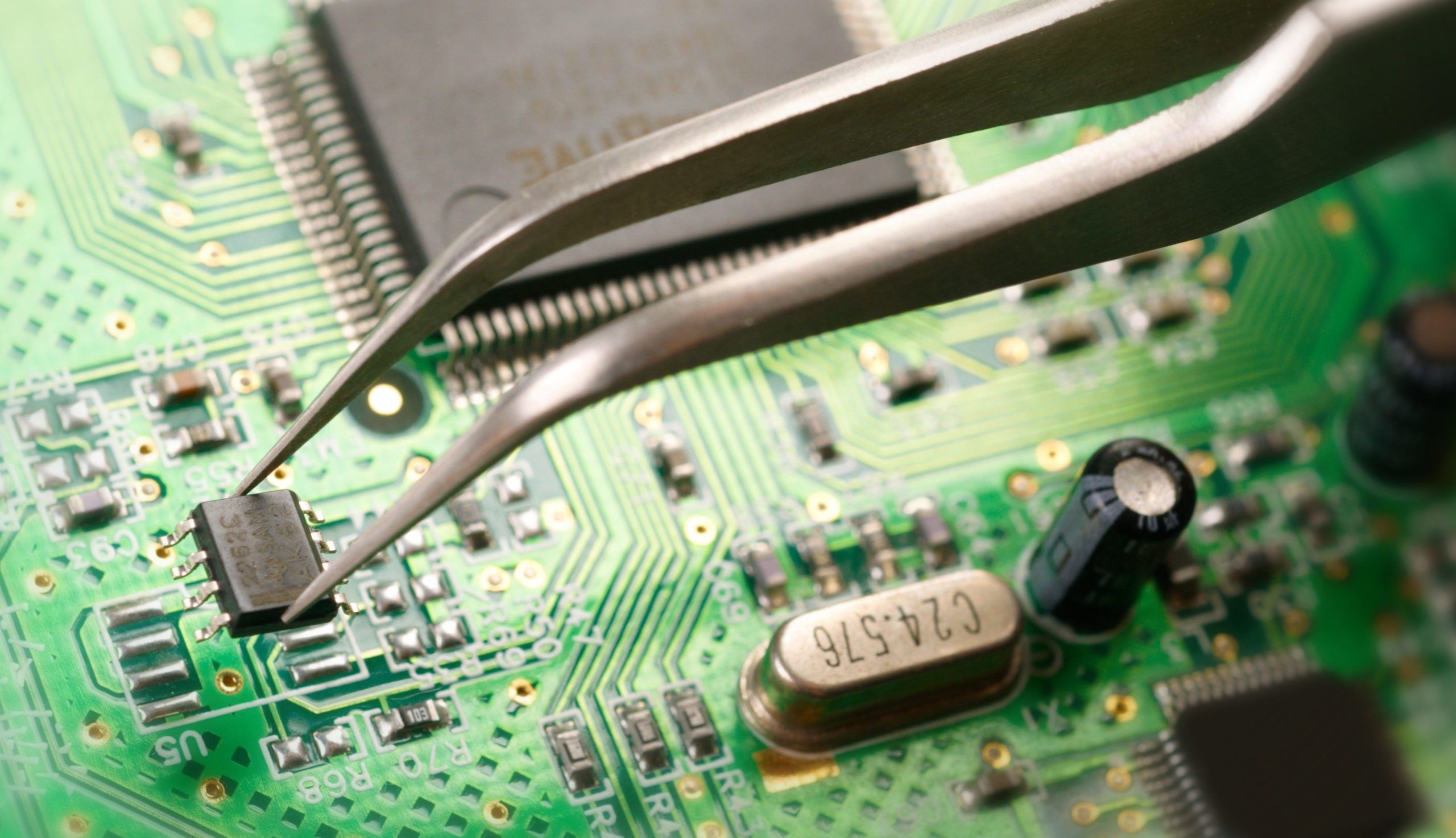
When troubleshooting a PCB, it’s essential to work systematically. Begin by inspecting the board visually for any obvious signs of damage, such as burned components or broken traces. Look for loose connections or components that are not properly seated. These visual inspections can often provide initial clues as to where the problem may lie.
Testing the power supply is another critical step in PCB troubleshooting. Use a multimeter or voltage tester to measure the voltages at various points on the board. Check for proper voltage levels and ensure that the power supply is stable and consistent. Many issues with PCBs can be traced back to faulty power supplies.
Circuit tracing and signal flow analysis are also important techniques in PCB troubleshooting. By tracing the path of a signal through the circuit, you can identify where it breaks down or encounters interference. This can be done using a logic analyzer or an oscilloscope.
Finally, don’t be afraid to consult resources and seek help from others when faced with a challenging PCB troubleshooting scenario. Online forums, manufacturer documentation, and experienced colleagues can provide valuable insights and solutions.
Electrical Testing Tools and Equipment for PCB Troubleshooting
Electrical Testing Tools and Equipment for PCB Troubleshooting
When it comes to troubleshooting PCBs, having the right set of electrical testing tools and equipment is essential. These tools not only help you identify the root cause of the issue but also enable you to test and verify the functionality of various components on the board. Here are some commonly used electrical testing tools for PCB troubleshooting:
Multimeter: A multimeter is a versatile tool that allows you to measure voltage, current, and resistance. It is invaluable for testing the continuity of traces, checking for short circuits, and verifying component values such as resistors and capacitors. Some advanced multimeters also have additional features like diode testing and frequency measurement.
Oscilloscope: An oscilloscope is a powerful tool for analyzing electronic signals in real-time. It allows you to visualize waveforms, measure voltage, and observe the behavior of signals at different points on the PCB. Oscilloscopes are particularly useful for troubleshooting issues related to timing, signal integrity, and noise.
Logic Analyzer: A logic analyzer is a specialized tool used to capture and analyze digital signals. It enables you to monitor multiple signals simultaneously and view their timing relationships. Logic analyzers are commonly used for troubleshooting problems in digital circuits, such as logic gates, microprocessors, and data communication interfaces.
Power Supply Tester: A power supply tester helps you verify the output voltage and current of a power supply unit. It ensures that the power supply is functioning within the specified limits and can provide a stable power source to the PCB. By using a power supply tester, you can quickly eliminate potential power supply issues as the cause of the problem.
Signal Generator: A signal generator is used to produce specific waveforms or frequencies. It is helpful for testing various circuit components and verifying their response to different input signals. Signal generators can simulate different scenarios, allowing you to assess the behavior of the PCB under different conditions.
IC Puller and IC Tester: An IC (integrated circuit) puller is a tool used to safely remove ICs from their sockets without damaging the PCB or the component. An IC tester, on the other hand, is used to test the functionality and performance of ICs. Both tools are essential for troubleshooting PCBs that use integrated circuits.
Having a well-equipped toolbox with these electrical testing tools not only speeds up the PCB troubleshooting process but also increases the accuracy of your diagnostic efforts. Familiarize yourself with the proper usage and functions of each tool to make the most of your troubleshooting endeavors.
Common Issues and Symptoms in PCBs
Common Issues and Symptoms in PCBs
Printed circuit boards (PCBs) can experience a variety of issues that affect their functionality and performance. Being aware of these common problems and their associated symptoms is crucial for effective troubleshooting. Here are some of the most prevalent issues you may encounter when working with PCBs:
Short Circuits: A short circuit occurs when two or more conductive elements on the PCB come into contact, bypassing the intended circuit path. Symptoms of a short circuit include sudden loss of power, unusual heating, and blown fuses. Short circuits can be caused by damaged components, improperly routed traces, or soldering defects.
Open Circuits: An open circuit is the opposite of a short circuit and happens when there is a break in the circuit path, preventing the flow of current. Intermittent or no power, unresponsive or malfunctioning components, and non-functional circuitry are common signs of open circuits. These can be caused by broken traces, loose connections, or faulty soldering.
Overheating Components: When certain components on a PCB become excessively hot, it indicates potential problems such as high current flow or inadequate heat dissipation. Overheating can lead to component failure, reduced lifespan, and performance issues. It can be caused by insufficient cooling, excessive current, or improper component selection.
Noise and Interference: Noise and interference can disrupt signals on a PCB, causing distorted or inaccurate data and affecting the overall performance of electronic devices. Symptoms include signal degradation, data corruption, and erratic behavior of components. Noise and interference can be introduced by improper grounding, electromagnetic interference (EMI), or proximity to other electronic devices.
Poor Solder Joints: Inadequate soldering can result in poor joints, which can lead to intermittent connections, loose components, and unreliable circuitry. Common signs of poor solder joints include intermittent functionality, component displacement, and visual inspection of dull or irregular solder joints. Proper soldering techniques and quality solder are essential to prevent these issues.
Component Failure: Components can fail due to various reasons, such as manufacturing defects, age, or excessive operating conditions. Failed components may exhibit symptoms like total power loss, abnormal behavior, or incorrect readings. Testing faulty components and replacing them is necessary to restore the functionality of the PCB.
By familiarizing yourself with these common issues and their symptoms, you can quickly identify and resolve problems in PCBs. It is important to approach troubleshooting systematically, starting with a visual inspection and expanding to more advanced diagnostic techniques using appropriate tools and equipment.
Circuit Tracing and Signal Flow Analysis
Circuit Tracing and Signal Flow Analysis
When troubleshooting PCBs, it is essential to have a thorough understanding of the circuit’s design and how signals flow through it. Circuit tracing and signal flow analysis are valuable techniques that help identify and resolve issues in a systematic manner.
Circuit Tracing: Circuit tracing involves following the path of a signal through the PCB to identify where it encounters issues or interruptions. This can be done using various tools such as a logic analyzer or an oscilloscope. By examining the input and output points of each component along the signal path, you can pinpoint the location of a potential problem.
When tracing a circuit, it is important to have a clear schematic diagram or layout of the PCB. This provides a visual reference and helps you understand the circuit’s intended path and connections. Additionally, using a multimeter in continuity mode can help identify broken traces or open circuits, ensuring the signal does not encounter any interruptions.
Signal Flow Analysis: Signal flow analysis involves analyzing how signals move through the circuit and how they interact with various components. This technique is particularly useful for diagnosing issues related to timing, noise, or signal integrity.
An oscilloscope is commonly used for signal flow analysis, allowing you to observe the waveform and measure the voltage at different points in the circuit. By comparing the expected signal behavior with the actual measurements, you can identify anomalies, such as distorted waveforms, excessive noise, or incorrect timing.
Signal flow analysis also involves testing individual components to ensure they are functioning correctly. This includes verifying the input and output signals of ICs, checking the resistance or capacitance of passive components, and examining the behavior of transistors or diodes. By systematically analyzing each component’s impact on the signal, you can identify faulty or malfunctioning parts.
Throughout the circuit tracing and signal flow analysis process, documenting your findings and observations is crucial. Take note of any abnormal behavior, measurements, or patterns that may be relevant to the troubleshooting process. These records can serve as a valuable reference for future diagnosis and will aid in maintaining an organized approach to troubleshooting.
Overall, circuit tracing and signal flow analysis are powerful techniques for diagnosing issues in PCBs. By understanding how signals move through the circuit and systematically examining components, you can efficiently identify and resolve problems, ensuring the functionality and performance of the PCB.
Visual Inspection and Component Testing
Visual Inspection and Component Testing
Visual inspection and component testing are fundamental techniques in PCB troubleshooting. They allow you to identify physical defects, loose connections, and faulty components that may be affecting the performance of the PCB. By combining visual inspection with targeted testing methods, you can efficiently diagnose and resolve issues.
Visual Inspection: Visual inspection involves carefully examining the PCB for any visible signs of damage or abnormalities. This includes inspecting components, solder joints, traces, and other elements on the board. Look for signs of burned or damaged components, loose connections, broken traces, or abnormal discoloration.
Pay close attention to solder joints, as poor soldering can result in open circuits or intermittent connections. Look for dull or irregular solder joints, which may indicate improper soldering techniques or insufficient solder flow. Additionally, check for any physical damage, such as bent or broken pins, cracked components, or excessive debris on the board.
Component Testing: Once the visual inspection is complete, component testing is essential to identify any faulty or malfunctioning parts. Use a multimeter or specialized component tester to check the resistance, capacitance, and functionality of various components on the PCB.
Begin by testing passive components such as resistors, capacitors, and inductors. Verify their values and ensure they are within the specified tolerance range. For active components like transistors, diodes, and integrated circuits, check their functionality by comparing the input and output signals with their expected values.
For ICs, it may be necessary to refer to the manufacturer’s documentation to understand the pin configuration and expected behavior. Test the ICs on a separate breadboard if possible to eliminate any other potential factors affecting their performance.
If you suspect a specific component is faulty, consider replacing it with a known working component to see if the issue is resolved. This process of substitution can help isolate the problem to a specific component or circuit section.
It is important to note that while visual inspection and component testing are effective techniques, they have limitations. They cannot always detect internal faults or intermittent issues that may arise due to temperature or other environmental factors. In such cases, more advanced diagnostic tools and techniques may be required.
By conducting a careful visual inspection and component testing, you can often identify and resolve issues in PCBs. These techniques serve as a starting point for troubleshooting, allowing you to narrow down the possible causes and focus your efforts on the areas that require further attention.
Troubleshooting Power Supply Issues in PCBs
Troubleshooting Power Supply Issues in PCBs
A well-functioning power supply is crucial for the proper operation of a printed circuit board (PCB). When power supply issues arise, it can cause a variety of problems, ranging from intermittent functionality to complete failure. Troubleshooting power supply issues requires a systematic approach to identify and resolve the underlying causes.
Visual Inspection: Begin troubleshooting by visually inspecting the power supply section of the PCB. Look for any signs of physical damage, such as burned components, bulging capacitors, or loose connections. Ensure that all power-related components, such as voltage regulators or transformers, are securely soldered and properly connected.
Check Voltage Levels: Use a multimeter to measure the voltage levels at various points in the power supply circuit. Compare the measured values with the expected values specified by the manufacturer or design specifications. Make note of any significant deviations, as they may indicate issues such as power fluctuations or component failures.
Verify Power Supply Stability: Ensure that the power supply is stable and providing a consistent output. Use an oscilloscope to check for any voltage ripple or fluctuation in the power signal. Excessive ripple or fluctuation can cause instability in the PCB’s operation and lead to malfunctions.
Inspect Power Supply Components: Thoroughly examine the power supply components, such as capacitors and voltage regulators, for any signs of damage or failure. Capacitors with bulging or leaking electrolyte should be replaced, as they can also cause power supply instability. Check the datasheets or specifications of the components to confirm their proper functioning.
Test Power Supply Connections: Check all the connections in the power supply circuit to ensure they are secure and making proper contact. Loose or improperly soldered connections can result in intermittent power supply issues. Pay close attention to power connector pins, as they can easily become loose or bent, impeding the flow of power.
Consider Load Testing: Load testing involves applying a simulated load to the power supply circuit to determine its performance under different conditions. This helps identify any voltage drops or fluctuations that may occur when the PCB is operating at maximum capacity or during specific tasks. Load testing can be done using load resistors or simulated loads specific to the PCB’s requirements.
Monitor Temperature: Excessive heat can affect the performance and stability of the power supply circuit. Ensure that the power supply components are not overheating and that there is adequate cooling in place. Insufficient cooling may cause thermal shutdowns or reduced power supply efficiency.
Consider Environmental Factors: External factors such as fluctuations in the mains voltage, electromagnetic interference (EMI), or poor grounding can also contribute to power supply issues. Evaluate the PCB’s environment and take necessary measures to mitigate these factors, such as installing EMI filters or ensuring proper grounding techniques.
By following these troubleshooting techniques, you can effectively identify and resolve power supply issues in PCBs. Once the underlying problems are addressed, the PCB should regain its functionality and operate reliably.
Identifying and Resolving Short Circuits
Identifying and Resolving Short Circuits
Short circuits are one of the most common issues that can occur in a printed circuit board (PCB). They happen when two or more conductive elements come into contact, creating an unintended path for current flow. A short circuit can cause a range of problems, from circuit malfunction to damage of components or the PCB itself. Therefore, it is crucial to promptly identify and resolve short circuits in PCBs.
Visual Inspection: Start by visually inspecting the PCB for any visible signs of short circuits. Look for components that may have been soldered incorrectly, resulting in a connection between adjacent traces or pads. Examine the board for any signs of physical damage, such as scratched traces or solder bridges.
Continuity Testing: Use a multimeter in continuity mode to check for electrical connections between points on the PCB that should not be connected. Place the multimeter probes on each end of a trace or a set of pads and verify that there is no continuity, indicating an open circuit. If there is continuity, it suggests the presence of a short circuit.
Isolation Testing: To pinpoint the location of a short circuit, use the isolation testing method. This involves disconnecting sections of the circuit and testing for continuity after each disconnection. Start by removing power and disconnecting components or sections of the circuit that are suspected to be the source of the short. Test for continuity after each disconnection until the short circuit is isolated.
Thermal Imaging: In some cases, a short circuit may generate heat due to excessive current flow. Using a thermal imaging camera, carefully examine the PCB for hotspots. These hotspots can indicate potential areas of short circuits or high resistance connections. The thermal image can help guide you to the location of the issue.
Short Circuit Removal: Once the short circuit is identified, the next step is to resolve it. If the short is caused by solder bridges, use a soldering iron and desoldering wick or vacuum tool to remove the excess solder and separate the connections. If the short is due to damaged traces, carefully cut the affected portion of the trace using a precision knife or a PCB repair kit. Then, create a new trace by soldering a thin wire between the two disconnected points.
Recheck for Short Circuits: After the repair, perform continuity testing or use a multimeter in resistance mode to confirm that the short circuit has been successfully resolved. Verify that there is no longer continuity where there shouldn’t be and that the resistance between previously shorted points has returned to values expected within the circuit design.
Preventative Measures: To minimize the occurrence of short circuits, some preventative measures can be taken during the PCB design and assembly process. These include adhering to proper spacing guidelines between traces and components, having good soldering practices, and performing thorough inspections before powering up the PCB.
By following these methods, you can effectively identify and resolve short circuits in PCBs. It is important to approach troubleshooting in a methodical manner and exercise caution to preserve the integrity of the PCB throughout the process.
Troubleshooting Open Circuits and Poor Connections
Troubleshooting Open Circuits and Poor Connections
Open circuits and poor connections are common issues that can occur in a printed circuit board (PCB). These problems can lead to intermittent functionality, complete loss of power, or unreliable circuit performance. Troubleshooting open circuits and poor connections requires a systematic approach to identify and resolve the underlying causes.
Visual Inspection: Begin by visually inspecting the PCB for any visible signs of open circuits or poor connections. Look for broken or damaged traces, loose or improperly soldered connections, and components that are not properly seated. Pay close attention to areas where wires or leads are connected to the PCB, such as connectors or headers.
Continuity Testing: Use a multimeter in continuity mode to test for continuity between points in the circuit that should be connected. Place one probe on one end of a trace or connection and the other probe on the other end. A lack of continuity indicates an open circuit or poor connection. Repeat this process for all critical connections in the circuit.
Inspect Solder Joints: Examine the quality of the solder joints on the PCB. Look for dull or irregular solder joints, which may indicate a poor connection. Use a magnifying glass or microscope, if necessary, to get a closer look at the solder joints. Ensure that there is proper solder flow and that the joint is free from any visible defects, such as solder balls or cold solder joints.
Reflow Soldering: If you suspect that poor connections are caused by inadequate soldering, reflow soldering may be necessary. This involves reheating the solder joints to reestablish proper connections. Use a soldering iron or hot air rework station to carefully heat the solder joints, ensuring that the proper soldering temperature is reached. Monitor the joints to ensure the solder reflows and establishes a strong connection.
Repair Broken Traces: If an open circuit is identified due to a broken trace, it will need to be repaired. Carefully scrape away any solder mask or protective coating around the break using a precision knife. Then, use a conductive ink pen or fine-gauge wire to create a bridge between the disconnected sections of the trace. Ensure that the repaired trace is securely attached and provides a continuous path for the current.
Ensure Proper Component Placement: Check that all components are properly seated and inserted in their respective sockets or connectors. Loose or improperly seated components can result in poor connections and intermittent functionality. Gently reseat any loose components, ensuring that they are correctly aligned and attached to their corresponding pins or pads.
Consider Connector Issues: Connectors can be a common source of poor connections due to loose pins, faulty contacts, or misalignment. Inspect the connectors and ensure that the pins or contacts are properly aligned and making adequate contact. Clean the contacts if they appear dirty or corroded, and consider replacing any connectors that are damaged or worn out.
By following these troubleshooting methods, you can effectively identify and resolve open circuits and poor connections in PCBs. It is important to approach troubleshooting in a systematic manner, inspecting and testing critical points in the circuit to ensure reliable connections and proper functionality.
Repairing PCB Traces and Pads
Repairing PCB Traces and Pads
Printed circuit boards (PCBs) can develop damaged or broken traces and pads over time due to various factors such as physical stress, improper handling, or manufacturing defects. These damaged traces and pads can result in connectivity issues or circuit malfunctioning. Repairing PCB traces and pads requires careful attention and precise techniques to ensure successful restoration of the circuit’s integrity.
Evaluate the Damage: Begin by carefully inspecting the damaged traces and pads on the PCB. Determine the extent of the damage and whether it is limited to the surface of the board or if it extends to inner layers. This will help you determine the appropriate repair method and assess the complexity of the repair.
Clean the Affected Area: Before proceeding with the repair, clean the affected area using an appropriate cleaning solution and a soft brush or cloth. This will help remove any debris, oxidation, or contaminants that may interfere with the repair process.
Wire Jumper: One common method for repairing open or broken traces is to use a wire jumper. This involves soldering a thin wire directly onto the trace, bridging the gap or reconnecting the broken sections. Use a wire with the appropriate gauge and material (e.g., copper or silver) to match the original trace width. Ensure proper soldering techniques to establish a secure and conductive bond between the wire jumper and the trace.
Conductive Epoxy or Ink: For more delicate repairs or areas where a wire jumper may not be suitable, conductive epoxy or ink can be used. Apply a small amount of the conductive epoxy or ink to bridge the gap or cover the damaged area of the trace. Allow sufficient time for the epoxy or ink to cure and harden, ensuring a stable electrical connection. Follow the manufacturer’s instructions for the specific product being used.
Pad Repair: Repairing damaged pads can be slightly more challenging. If the pad is partially damaged, you can carefully scrape away any residual solder mask or debris using a precision knife. This will expose a clean area of the pad for subsequent repair. Follow the same wire jumper or conductive epoxy/ink method mentioned earlier to establish a new connection on the repaired pad.
Pad Replacement: In the case of severely damaged or heavily corroded pads, pad replacement may be necessary. This involves carefully removing the damaged pad using a desoldering tool or hot air rework station, ensuring not to damage the surrounding components or traces. Once the damaged pad is removed, a new pad can be soldered in its place. This replacement pad can be a commercially available replacement or a custom-made pad fabricated using appropriate techniques and materials.
Inspect and Test: After the repair is completed, perform a thorough inspection of the repaired area to ensure that the connections are secure and free from any short circuits or unintended connections. Use a multimeter or continuity tester to verify the resistance and conductivity of the repaired traces and pads. This will help ensure the successful restoration of the circuit’s functionality.
By following these techniques, you can repair damaged traces and pads on a PCB, restoring connectivity and ensuring proper functionality. It is important to exercise caution and precision during the repair process to prevent further damage and maintain the integrity and reliability of the repaired PCB.
Troubleshooting Logic and Data Communication Issues
Troubleshooting Logic and Data Communication Issues
Logic and data communication issues can result in circuit malfunction or data corruption in printed circuit boards (PCBs). These issues can arise due to a variety of factors, including incorrect programming, faulty components, or improper signal transmission. Effective troubleshooting of logic and data communication issues requires a systematic approach to identify and resolve the underlying causes.
Review the Circuit Design: Begin by reviewing the circuit design and documentation to ensure that it aligns with the intended functionality and specifications. Verify that the connections, logic gates, microcontrollers, and other components are correctly implemented according to the circuit’s design. Any discrepancies or errors in the design can lead to logic and data communication issues.
Functional Testing: If the circuit has a specific function or expected output, perform functional testing to verify whether the desired results are being achieved. This can involve inputting specified signals or data and comparing the actual output with the expected output. By identifying any disparities, you can narrow down the potential causes of the logic or data communication issue.
Data Flow Analysis: Analyze the flow of data through the circuit or communication pathway. Trace the data path from the source to the destination, checking each stage or component along the way. Verify that the data is being transmitted correctly, and search for any points where the data flow may be disrupted or corrupted.
Signal Integrity Analysis: Check the quality and integrity of the signals being transmitted. Use an oscilloscope or logic analyzer to observe the waveforms or digital signals at various points in the circuit. Look for any abnormalities such as noise, distortions, or unexpected signal levels. These issues can indicate problems with signal transmission, incorrect voltage levels, or interference.
Verify Component Functionality: Test the individual components involved in the logic or data communication process. Evaluate the functionality of microcontrollers, logic gates, transceivers, or any other relevant components. Ensure that they are properly programmed or configured and that they are operating within their specified parameters.
Check Wiring and Connections: Inspect the wiring and connections in the circuit or data communication pathway. Examine the physical connections, such as cables, connectors, or soldered joints, for any signs of damage, loose or bent pins, or poor soldering. Validate that the connections are secure and compatible with the required signal transmission rates.
Software Analysis: If the logic or data communication issue is related to software or firmware, analyze the code or programming. Check for any logical errors, incorrect configurations, or software bugs that may be affecting the desired behavior. Debugging tools and techniques can help identify and resolve software-related issues.
Collaborate and Seek Expertise: If the troubleshooting efforts become challenging or inconclusive, it can be helpful to collaborate with colleagues or seek assistance from experts in the field. Online forums, technical support from component manufacturers, or specialized consultants can provide valuable insights and guidance for resolving complex logic and data communication issues.
By following a systematic troubleshooting approach and employing the appropriate tools and techniques, you can effectively identify and resolve logic and data communication issues in PCBs. It is essential to consider all possible factors, including circuit design, components, signals, and software, to ensure the proper functionality and integrity of the circuit or data communication system.
Soldering and Desoldering Techniques for PCB Repair
Soldering and Desoldering Techniques for PCB Repair
Soldering and desoldering are critical skills for repairing and modifying printed circuit boards (PCBs). Whether replacing components, fixing broken connections, or making circuit modifications, properly executing these soldering and desoldering techniques is essential for a successful repair. Here are some key techniques to master.
Soldering:
1. Prepare the Board: Clean the PCB and ensure that the soldering area is free from dust, dirt, or debris. It is also important to have a well-ventilated workspace and appropriate safety equipment such as safety goggles and heat-resistant gloves.
2. Select the Right Tools: Use a temperature-controlled soldering iron suitable for electronics work. A fine-tipped soldering iron is ideal for precision soldering. Additionally, choose a solder with a suitable diameter and composition (typically a lead-based or lead-free solder, depending on your needs).
3. Heat Management: Preheat the soldering iron to the proper temperature for the specific solder and component you are working with. It is crucial not to apply too much heat for too long as this can damage sensitive components or the PCB itself. Apply the heated iron to the joint and the component lead simultaneously and introduce the solder to create a secure bond.
4. Good Solder Joint: Create neat and reliable solder joints by ensuring that the solder flows smoothly around the component lead and the PCB pad. The joint should have a shiny appearance and form a smooth fillet around the pad and lead. Avoid creating solder bridges or excess solder, as these can lead to short circuits or poor connections.
Desoldering:
1. Prepare the Board: Clean the PCB and clear the soldering area of any excess solder, debris, or components. Make sure the desoldering area is clear and accessible.
2. Select the Right Tools: Have a desoldering pump or a desoldering wick on hand. The desoldering pump uses suction to remove molten solder, while desoldering wick (also known as solder wick) absorbs the solder effectively.
3. Heat Management: Heat the solder joint with a soldering iron until the solder melts. Place the tip of the desoldering pump or the desoldering wick onto the molten solder. Activate the pump to create suction or press the wick onto the solder to absorb it. Remove both the desoldering pump or the wick and the soldering iron simultaneously before the solder solidifies again.
4. Clean and Inspect: After desoldering, clean the area to remove any residual flux or debris left behind. Inspect the PCB and component leads for any damage or lifted pads that may require repair.
Practicing these soldering and desoldering techniques is vital to become proficient in PCB repair. It is advisable to practice on old or discarded PCBs before working on important projects, as this will allow you to refine your skills and gain confidence.
Dealing with Electrostatic Discharge (ESD) and Static Electricity
Dealing with Electrostatic Discharge (ESD) and Static Electricity
Electrostatic discharge (ESD) and static electricity pose significant risks to sensitive electronic components and printed circuit boards (PCBs). Even a small discharge of static electricity can damage or destroy components, leading to circuit malfunction or failure. It is essential to be aware of these risks and take appropriate measures to mitigate ESD and static electricity during PCB handling and repair processes.
Understanding ESD: ESD occurs when there is a rapid transfer of an electric charge between two objects at different electrical potentials. The discharge can generate voltages in thousands of volts, with minimal human perception. ESD can damage or degrade electronic components, leading to latent failures or immediate damage.
Preventive Measures:
- Ground Yourself: Before working with PCBs, establish a grounding connection by wearing an ESD grounding wrist strap or using an ESD mat. These devices ensure that any static charge you may carry is safely discharged to a grounded source.
- Work in an ESD-Safe Area: Set up your workspace in an ESD-safe area with ESD dissipative flooring and workbenches. These surfaces help prevent the buildup and discharge of static charges. Additionally, use conductive bins, trays, and storage containers designed to minimize static electricity.
- Proper PCB Handling: Handle PCBs by their edges or designated grip areas to minimize contact with sensitive components. Avoid touching exposed contacts or traces, as oils and contaminants from your fingers can contribute to static build-up.
- Anti-Static Packaging: Keep PCBs and components in anti-static containers or packaging until they are ready to be installed. These materials provide a protective shield against static charges and reduce the risk of ESD-related damage.
Safe Work Practices:
- Avoid Working in Dry Environments: Dry environments encourage the build-up of static charges. Control humidity levels in the work area, as higher humidity helps dissipate static electricity.
- Minimize Movement: Rapid movements and friction can generate static charges. Minimize unnecessary movement and do not shuffle your feet on carpets or rugs, as these actions can potentially generate a high-static charge.
- Proper Tool Usage: Use ESD-safe tools when working with sensitive components or PCBs. These tools are designed to discharge static electricity and prevent ESD-related damage. Invest in quality soldering irons with grounded tips to minimize the risk of ESD during soldering or desoldering.
ESD-Safe Work Environment:
- Regular ESD Control Audits: Establish a regular audit and maintenance schedule to ensure that all ESD control measures, like wrist straps, grounding connections, and ESD-safe equipment, are in good working order and correctly used.
- Training and Awareness: Educate all personnel who handle PCBs about the risks of ESD and safe handling procedures. Provide proper training on ESD control measures and emphasize the importance of adhering to ESD-safe practices.
- Special Handling for Highly Sensitive Components: Some components are exceptionally sensitive to ESD. Take extra precautions when working with these devices, such as using specialized handling equipment, anti-static storage containers, and extreme care during installation.
By following these guidelines, you can significantly reduce the risk of ESD and static electricity-related damage to PCBs and electronic components. Implementing appropriate ESD control measures and maintaining an ESD-safe work environment are essential to ensure the integrity and proper functioning of electronic devices.
Troubleshooting Common EMI/EMC Problems in PCBs
Troubleshooting Common EMI/EMC Problems in PCBs
Electromagnetic Interference (EMI) and Electromagnetic Compatibility (EMC) issues can significantly impact the performance and reliability of printed circuit boards (PCBs). EMI refers to the unwanted electromagnetic energy that interferes with the normal operation of electronic circuits. EMC, on the other hand, focuses on designing and ensuring that a PCB functions properly in its intended electromagnetic environment. Troubleshooting EMI/EMC problems in PCBs requires a systematic approach to identify and resolve the underlying causes.
Identify Potential Sources:
Begin by identifying potential sources of EMI, both internal and external to the PCB. Internal sources can include switching power supplies, high-speed digital circuits, or improperly grounded components. External sources may be nearby electronic devices, power lines, or wireless communication systems. Identify potential troublemakers that generate or receive significant electromagnetic energy.
Shielding and Grounding:
Ensure proper grounding throughout the PCB to minimize the impact of EMI. This involves connecting all grounding points together and providing a path to earth ground. Implement shielding techniques, such as using conductive enclosures or shields, to contain electromagnetic energy and prevent interference from entering or leaving the PCB.
Trace Routing and Layout:
Poorly designed PCB traces can act as antennas, propagating unwanted electromagnetic waves or cross-talking signals. Analyze the routing and layout of traces, paying attention to high-speed signal paths, sensitive analog circuits, and power lines. Keep traces as short as possible and separate high-speed and low-frequency signals. Use proper ground planes and ensure that signal return paths are clear and direct.
Component Placement:
Component placement plays a crucial role in minimizing EMI/EMC issues. Place sensitive components away from potential noise sources and high-power components that may emit electromagnetic radiation. Follow design guidelines from component manufacturers and ensure proper spacing and isolation between components and traces to reduce crosstalk and interference.
Filtering and Decoupling:
Use appropriate filtering and decoupling techniques to suppress noise and ripple on power lines. Adding decoupling capacitors across power supply pins of integrated circuits and placing ferrite beads or inductors on signal lines can help attenuate high-frequency noise and reduce EMI. Implementing filters on input/output lines, such as common-mode chokes or RC filters, can also mitigate unwanted electromagnetic emissions.
Testing and Validation:
Perform comprehensive laboratory testing to assess the PCB’s electromagnetic performance. Use EMI measurement instruments, such as spectrum analyzers or near-field probes, to identify electromagnetic emissions and their sources. Conduct EMI/EMC compliance testing by following applicable standards and regulations to ensure that the PCB meets the required electromagnetic compatibility specifications.
Simulation and Modeling:
Use electromagnetic simulation software to model and analyze the behavior of the PCB design. Simulations can help identify potential EMI/EMC issues early in the design phase, enabling you to make necessary adjustments to reduce electromagnetic emissions and susceptibility. Analyzing simulations can also aid in assessing the effectiveness of potential design changes or mitigation strategies.
By employing these troubleshooting techniques, you can successfully address EMI/EMC problems in PCBs. It is important to approach EMI/EMC design and troubleshooting with care, following best practices and considering specific requirements for the intended application and industry standards.
Software Tools and Techniques for PCB Troubleshooting
Software Tools and Techniques for PCB Troubleshooting
Software tools can greatly enhance the effectiveness and efficiency of PCB troubleshooting. They provide valuable insights into the functioning of the circuit, help diagnose issues, and aid in resolving problems. Here are some commonly used software tools and techniques for PCB troubleshooting:
Circuit Simulation Software: Circuit simulation software allows designers and troubleshooters to virtually model and simulate the behavior of a PCB design. By inputting the circuit parameters, component values, and signal characteristics, simulation tools can provide valuable information about circuit performance, signal integrity, and potential sources of issues. Simulation software enables the identification of weak points, helps optimize circuit performance, and speeds up the troubleshooting process.
PCB Design Software: PCB design software not only assists in creating layouts but also provides tools for troubleshooting. For example, these tools can perform design rule checks (DRC) to identify potential issues, such as incorrect component placement, trace clearance violations, or overlapping polygons. By running DRC checks, you can catch and correct errors early, helping to prevent unnecessary troubleshooting and rework.
Data Analysis Software: Data analysis software can be a valuable asset for troubleshooting complex systems. These tools are especially useful when dealing with data communication or signal processing issues. By analyzing the data collected from sensors, communication modules, or control circuits, data analysis software can help identify patterns, correlations, and anomalies. These insights can aid in troubleshooting and pinpointing the root cause of issues within the PCB or the system it is embedded in.
Logic Analyzer and Oscilloscope Software: Logic analyzer and oscilloscope software tools are used to capture, analyze, and visualize electronic signals in real-time. By connecting the target PCB to the software, these tools provide a detailed view of signal waveforms, timing relationships, and voltage levels. With advanced triggering options and protocol-specific decoding capabilities, logic analyzer and oscilloscope software can help troubleshoot complex digital circuits, verify data communication protocols, and debug intricate timing issues.
Bill of Materials (BOM) Management Software: BOM management software helps organize and track the components used in a PCB design. By maintaining an up-to-date BOM, you can ensure that the correct components are sourced and installed. This software also assists in identifying component substitutes, checking for component availability, and managing revisions. Proper BOM management can prevent troubleshooting delays caused by incorrect or out-of-stock components.
Collaboration and Documentation Tools: Collaboration platforms and documentation tools facilitate effective communication and knowledge sharing among team members involved in PCB troubleshooting. Online platforms allow team members to share project files, capture design changes, and discuss issues in real-time. Documentation tools help maintain accurate records of troubleshooting activities, including notes, annotations, and images. These tools streamline team collaboration and help maintain an organized troubleshooting workflow.
Integrating these software tools and techniques into the PCB troubleshooting process can greatly enhance the ability to diagnose and resolve issues efficiently. The use of software tools allows for a comprehensive analysis of the PCB design and its performance, enabling troubleshooters to gain deeper insights into the system’s behavior and make informed decisions for resolution.
Collaborating and Seeking Help for Difficult PCB Troubleshooting Scenarios
Collaborating and Seeking Help for Difficult PCB Troubleshooting Scenarios
When faced with difficult PCB troubleshooting scenarios, collaboration and seeking help can be invaluable. The complexity of modern electronic systems often requires the expertise and insights of multiple individuals to diagnose and resolve intricate issues. Here are some key considerations when collaborating and seeking help for difficult PCB troubleshooting scenarios:
Team Collaboration:
Encourage collaboration among team members involved in PCB troubleshooting. Establish open lines of communication to facilitate the sharing of knowledge, insights, and experiences. Regularly scheduled team meetings or brainstorming sessions can provide a platform for discussing challenging scenarios, exchanging ideas, and seeking input from colleagues.
Consulting Experts:
When facing particularly challenging PCB troubleshooting scenarios, it may be necessary to consult experts in the field. Seek advice from experienced individuals or specialized consultants who have extensive knowledge and expertise in the specific areas of concern. Experts can provide valuable insights, alternative perspectives, and practical solutions to resolve complex issues.
Online Forums and Communities:
Participate in online forums and communities dedicated to PCB troubleshooting and electronics. These platforms foster collaboration and knowledge sharing among professionals and enthusiasts. Pose specific questions or describe the symptoms you’re experiencing to seek guidance from the community. Online forums allow you to tap into a wide range of experiences and perspectives that can help pinpoint the root cause of the problem or suggest potential solutions.
Manufacturer Support:
Reach out to component manufacturers for technical support and guidance. Many manufacturers offer online resources, knowledge bases, and support forums. They have experts who can provide insight into specific component behavior, product specifications, or troubleshooting techniques. Manufacturer support is particularly valuable when dealing with component-related issues or when seeking clarification on datasheet information.
Technical Literature and Research:
Delve into technical literature, research papers, and industry publications related to the specific issues you are facing. The knowledge gained from these resources can provide valuable insights into best practices, case studies, and troubleshooting methodologies. Staying abreast of the latest research and industry developments can enhance your ability to diagnose and resolve difficult PCB troubleshooting scenarios.
Documentation and Record Keeping:
Maintain meticulous documentation throughout the troubleshooting process. Record observations, test results, experiments, and all attempted solutions. Documenting troubleshooting steps and their outcomes provides a historical record of the progress made, helps identify patterns or trends, and allows for iterative improvements. Accurate documentation also helps when collaborating with colleagues or seeking help from external sources.
In difficult PCB troubleshooting scenarios, collaboration and seeking help are essential for effectively resolving complex issues. Embracing collaboration, accessing various resources, and seeking expertise outside of your immediate circle can bring fresh insights, alternative perspectives, and innovative solutions to overcome challenges and achieve successful outcomes.