
Definition of DIP
The term DIP stands for Dual Inline Package. It is a type of electronic component package that is widely used in the electronics industry for integrated circuits (ICs), microcontrollers, and other semiconductor devices. DIPs are named as such because they have two rows of pins or leads that extend from the bottom of the package, making a “dual inline” configuration.
DIPs are typically made of a molded plastic body with a rectangular shape, although ceramic packages are also sometimes used. The pins or leads are evenly spaced along both sides of the package, with a standard spacing of 0.1 inches (2.54mm) between each pin. This spacing allows for easy insertion into a printed circuit board (PCB) and provides a standardized interface for connecting the component to other circuitry.
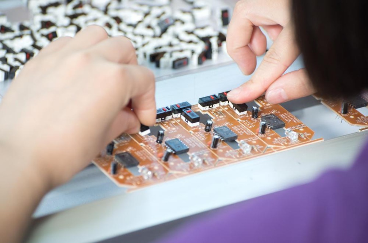
One of the key characteristics of DIPs is their through-hole design. This means that the pins extend through the bottom of the package and are soldered onto the PCB, providing a secure and reliable electrical connection. The through-hole mounting method is particularly advantageous for applications where mechanical stability and resistance to vibration are important.
DIPs are available in various pin configurations, ranging from as few as 8 pins to as many as several hundred pins. The number of pins depends on the complexity of the integrated circuit or device housed within the package. Common pin configurations include DIP-8, DIP-16, DIP-28, and DIP-40, among others.
DIPs were widely used in electronics manufacturing during the 1970s and 1980s but have gradually been replaced by smaller and more advanced surface mount technology (SMT) packages. Nonetheless, DIPs are still commonly used in applications where larger pin counts, higher power dissipation, and durability are required.
Overall, the DIP package provides a straightforward and reliable means of housing and connecting integrated circuits and other semiconductor devices. Its standardized pin configuration and through-hole design have made it a popular choice for numerous electronic applications over the years.
Structure and Design of DIP
The structure and design of a Dual Inline Package (DIP) play a crucial role in its functionality and versatility. Understanding the key components of a DIP can help in better utilizing its capabilities in various electronic applications.
A DIP mainly consists of three main parts: the plastic or ceramic body, the pins or leads, and the integrated circuit (IC) encapsulated within.
The plastic body of a DIP is typically rectangular in shape and made from a durable and heat-resistant material. It provides protection to the delicate IC inside and helps in dissipating heat generated during operation. In some cases, ceramic packages are used instead of plastic, offering better electrical insulation and thermal conductivity.
The pins or leads of a DIP are the contact points that extend from both sides of the package. These pins are usually made of metal, such as brass or copper, and spaced apart evenly with a standard pitch of 0.1 inches (2.54 mm). The spacing between the pins is critical as it allows for easy insertion into a printed circuit board (PCB) and ensures proper alignment and connectivity.
In addition to the standard DIP configuration, there are other variations available, including zigzag, gull-wing, and J-leaded designs. These variations offer different pin arrangements and are often used for specific applications where space constraints or specific mounting requirements exist.
The integrated circuit (IC) within a DIP is the heart of the package and contains the electronic components, such as transistors, resistors, and capacitors, necessary for the desired functionality. The IC is encapsulated within the plastic or ceramic body using specialized techniques to ensure electrical insulation and protection against external elements.
Furthermore, different DIP packages support specific numbers of pins, depending on the complexity of the IC housed within. Common pin configurations for DIPs include 8, 16, 28, and 40 pins, among others. This variety allows for different IC designs and accommodates a wide range of applications.
The structure and design of a DIP make it a versatile and widely used package in electronics manufacturing. Its simplicity, standardized pin configuration, and through-hole mounting method have contributed to its longevity in the industry. While surface mount technology (SMT) and smaller packages have gained popularity, DIPs remain significant in applications where larger pin counts, heat dissipation, and mechanical stability are essential.
Applications of DIP
The Dual Inline Package (DIP) is a versatile electronic component package that finds application in a wide range of industries and devices. Its simple design and reliable connectivity make it suitable for numerous electronic circuits and systems. Let’s explore some of the common applications of DIP:
1. Integrated Circuits (ICs): DIP packages are widely used to house ICs, including microcontrollers, programmable logic devices, digital signal processors, and memory chips. These ICs are vital components in various electronic devices, such as computers, smartphones, consumer electronics, automotive systems, and industrial equipment.
2. Printed Circuit Boards (PCBs): DIPs are easily mounted onto PCBs due to their through-hole design. They serve as the primary interface between the ICs and the PCB, allowing for efficient signal transmission and reliable connections. Many DIPs can be soldered directly onto the PCBs, ensuring excellent mechanical stability.
3. Power Electronics: DIP packages with higher pin counts are commonly used for power electronics applications. These include components like power amplifiers, voltage regulators, motor controllers, and solid-state relays. The through-hole mounting provides better heat dissipation, reducing the risk of overheating and ensuring safe and efficient power transfer.
4. Industrial Control Systems: DIP packages are prevalent in various industrial control systems, such as programmable logic controllers (PLCs), factory automation equipment, and robotics. These systems require reliable and durable components, and DIP packages, with their robust construction and standardized pin configurations, meet those requirements.
5. Communication Systems: DIP packages find application in communication devices, including modems, routers, network switches, and wireless transceivers. These devices rely on integrated circuits for data transmission, signal processing, and network connectivity. DIP packages offer a stable electrical connection and ensure the efficient operation of communication systems.
6. Automotive Electronics: DIP packages are used in various automotive systems, from engine control units (ECUs) and airbag control modules to infotainment systems and lighting controls. The mechanical stability and reliability of DIP packages make them suitable for the demanding and harsh environments encountered in automotive applications.
7. Laboratory Equipment: DIP packages are commonly used in laboratory equipment, such as oscilloscopes, function generators, power supplies, and multimeters. These instruments rely on integrated circuits to perform accurate measurements, signal generation, and data analysis. The through-hole design of DIP packages ensures secure connections and minimizes signal interference.
8. Educational Electronics: DIP packages are frequently utilized in educational settings for teaching electronics and circuit design. They allow students to understand the fundamentals of electronic circuits and provide a platform for hands-on experiments and prototyping. DIP packages offer a convenient interface for connecting components and sensors.
These are just a few examples of the wide-ranging applications of DIP packages across various industries. The simplicity, reliability, and versatility of DIPs make them an enduring choice for circuit designers and engineers seeking a robust and cost-effective solution for their electronic devices and systems.
Advantages and Disadvantages of DIP
The Dual Inline Package (DIP) has been a widely used electronic component package for several decades. While DIP packages offer various advantages, they also come with a few limitations. Understanding these advantages and disadvantages is important when considering DIPs for electronic applications. Let’s explore them below:
Advantages of DIP:
- Robust Construction: DIP packages are known for their sturdy design, which provides durability and mechanical stability. This makes them suitable for applications where resistance to vibration and shocks is important, such as automotive electronics and industrial control systems.
- Through-Hole Mounting: DIP packages feature through-hole leads that extend from the bottom of the package. This allows for easy insertion and secure soldering onto printed circuit boards (PCBs), ensuring reliable electrical connections. Through-hole mounting also simplifies troubleshooting and repair processes.
- Standardized Pin Configuration: DIP packages have a standardized pin spacing of 0.1 inches (2.54 mm). This makes it easier to design and manufacture PCBs, as the pins can be aligned to match the standard grid pattern. Additionally, the standardization facilitates component interchangeability and simplifies circuit designs.
- Higher Power Dissipation: DIP packages with larger pin counts have better power dissipation capabilities compared to smaller surface mount packages. This makes them ideal for power electronics applications, where components may generate significant heat during operation.
- Ease of Prototyping: DIP packages are widely available, making them readily accessible for prototyping and experimentation. Their compatibility with breadboards and development boards allows engineers and hobbyists to quickly prototype and validate their designs prior to mass production.
Disadvantages of DIP:
- Larger Physical Size: DIP packages tend to have larger footprints compared to smaller surface mount packages. This can be a disadvantage when space constraints are a concern, especially in compact electronic devices where miniaturization is crucial.
- Limited Pin Count: While DIP packages are available in various pin configurations, they have a limited maximum pin count compared to some surface mount packages. This can be a limitation when designing complex circuits that require a large number of connections.
- Lack of Component Variety: With the shift towards surface mount technology, the availability of new integrated circuits in DIP packages has decreased. Many advanced and specialized components are now only available in surface mount packages, limiting the options for designs that specifically require DIPs.
- Limited Application in High-Frequency Circuits: DIP packages may not be suitable for high-frequency applications due to their relatively longer lead lengths, which can introduce unwanted signal losses and increased inductance. Surface mount packages are typically preferred for such circuits.
Despite their disadvantages, DIP packages continue to be utilized in numerous applications where their advantages outweigh the limitations. The choice to use DIPs ultimately depends on the specific requirements of the project, including the available space, power dissipation needs, and desired level of prototyping convenience.
Differences Between DIP and Other Electronic Components
The Dual Inline Package (DIP) is just one type of electronic component package among many others available in the market. Each package type has its own unique characteristics, applications, and advantages. Let’s explore the differences between DIP and some commonly used electronic component packages:
DIP vs. Surface Mount Technology (SMT):
- Mounting Method: DIP packages use through-hole mounting, where the pins are inserted through holes in the PCB and soldered on the opposite side. SMT packages, on the other hand, are mounted directly on the surface of the PCB, without the need for through-hole soldering.
- Size and Space Requirements: DIP packages are generally larger in size compared to SMT packages, which allows for easier handling and prototyping. SMT packages, on the other hand, have smaller footprints and offer greater space efficiency, making them suitable for compact electronic devices.
- Component Variety: DIP packages have a limited selection of new and advanced components available, as many manufacturers are focusing on developing SMT packages. SMT packages offer a wider range of components, including microcontrollers, integrated circuits, resistors, capacitors, and more.
- Heat Dissipation: DIP packages, with their through-hole design, provide better heat dissipation capabilities compared to SMT packages. The through-hole leads act as a conduit for heat transfer, making DIPs more suitable for high-power applications.
- Manufacturing and Cost: SMT technology has gained popularity due to its automated assembly processes and higher production volumes, resulting in lower manufacturing costs. DIP packages, especially those with larger pin counts, require manual soldering and may have slightly higher manufacturing costs.
DIP vs. Ball Grid Array (BGA):
- Pin Configuration: DIP packages have pins that extend from both sides of the package, while BGA packages feature an array of solder balls on the bottom surface, providing a high pin count in a compact form.
- Electrical Performance: DIP packages, with their through-hole leads, may introduce parasitic effects such as inductance and capacitance, which can impact high-frequency performance. BGA packages are better suited for high-frequency applications due to their shorter interconnections and reduced parasitics.
- Soldering Method: DIP packages require manual soldering, while BGA packages are typically soldered using automated assembly techniques, such as reflow soldering, which offers better consistency and reliability.
- Thermal Considerations: DIP packages have a larger surface area, providing better heat dissipation capabilities compared to BGA packages. BGA packages may require additional thermal management solutions, such as heat sinks or thermal vias, to ensure optimal performance.
- Application Specifics: DIP packages are often preferred for prototyping, testing, and educational purposes due to their ease of use and availability. BGA packages are commonly used in high-performance applications such as graphics processing units (GPUs), advanced processors, and memory modules.
There are many other electronic component packages available, each with its own set of advantages and application-specific use cases. Choosing the right package type depends on factors such as space requirements, electrical performance, manufacturing processes, and project-specific needs.
Popular Types of DIP Packages
The Dual Inline Package (DIP) is available in various configurations to accommodate different pin counts and component types. Let’s explore some of the popular types of DIP packages:
1. DIP-8: The DIP-8 package is one of the most common types of DIP packages, featuring eight pins. It is frequently used for operational amplifiers, comparators, and other simple integrated circuits.
2. DIP-16: The DIP-16 package is widely used for a range of integrated circuits requiring more pin connections. It is commonly found in microcontrollers, digital-to-analog converters, and analog-to-digital converters.
3. DIP-28: The DIP-28 package is commonly used for more complex integrated circuits, such as microprocessors, memory chips, and programmable logic devices. It offers a higher pin count for increased functionality.
4. DIP-40: The DIP-40 package is a larger form factor DIP package that supports higher pin counts. It is often used for microcontrollers, analog ICs, and other applications requiring more extensive connections.
5. Zigzag DIP: Zigzag DIP packages are designed to reduce the packaging footprint by staggering the pins in a zigzag pattern, allowing for closer spacing between pins. This type of DIP package is commonly used in compact electronic devices where space is limited.
6. Gull-wing DIP: Gull-wing DIP packages have their leads bent outward in a “gull-wing” shape. This configuration allows for easier visual inspection and automated soldering during the assembly process. Gull-wing DIPs are commonly used in surface mount technology (SMT) applications.
7. J-leaded DIP: J-leaded DIP packages have leads that extend in a “J” shape, providing more stability and improved solder joint integrity. They are commonly used for high-reliability applications where mechanical stress and vibration resistance are important factors.
8. SIP (Single Inline Package): Although not strictly a DIP package, the SIP format is worth mentioning. SIP packages feature a single row of pins rather than the dual inline configuration. They are often used for linear integrated circuits and provide a space-saving alternative to DIP packages.
These are just a few examples of the popular types of DIP packages available. The specific choice of DIP package depends on the requirements of the integrated circuit or component being used, including the required pin count, space availability, and the desired level of mechanical stability.
How to Use DIP in Circuit Design
Integrating a Dual Inline Package (DIP) into a circuit design requires careful consideration and proper implementation. Here are some essential steps to effectively use DIP packages in circuit design:
1. Component Selection: Identify the specific DIP package that meets the requirements of your circuit design, such as the pin count, package size, and compatibility with the targeted application. Ensure that the chosen DIP package is readily available and supported by the manufacturer.
2. Pin Mapping: Study the datasheet of the integrated circuit (IC) to understand the pin functions and electrical characteristics. Determine the pin connections required for your circuit design and create a pin map or schematic diagram of the DIP package. This will serve as a reference during the PCB layout process.
3. PCB Layout: Place the DIP package appropriately on the PCB layout, aligning the pins with the corresponding pads on the PCB. Follow the pin map to ensure correct connectivity. Pay attention to pin spacing and orientation to avoid layout errors. Leave sufficient space around the DIP package for soldering and easy access during assembly.
4. Trace Routing: Route the PCB traces to interconnect the pins of the DIP package with other components and circuitry on the board. Ensure that the traces are properly sized to handle the required current and minimize noise interference. Follow good PCB design practices, such as avoiding sharp corners and crossing of traces to improve signal integrity.
5. Thermal Considerations: If the DIP package dissipates significant heat, ensure that the PCB layout and surrounding components allow for proper heat dissipation. Use thermal vias or heat sinks if necessary to maintain the temperature within acceptable limits.
6. Soldering: When soldering the DIP package onto the PCB, ensure proper alignment and contact between the pins and pads. Apply good soldering techniques, such as preheating the PCB, using the appropriate soldering iron temperature, and inspecting the solder joints for proper wetting and filleting.
7. Testing and Troubleshooting: After the DIP package is soldered onto the PCB, perform thorough testing to ensure proper functionality of the circuit. Use suitable testing equipment, such as multimeters and oscilloscopes, to verify signal integrity and functionality. Troubleshoot any issues that arise, checking for potential soldering, wiring, or component compatibility problems.
8. Documentation: Document the details of the DIP package used in the circuit, including the part number, pin map, and any specific considerations or modifications made during assembly. This documentation will be helpful for future reference, troubleshooting, and future circuit designs based on similar requirements.
By following these steps, you can effectively incorporate DIP packages into your circuit design, ensuring proper connectivity, functionality, and reliability. Proper attention to detail during component selection, layout, soldering, and testing will help optimize the performance and longevity of your circuit design.
Potential Issues and Troubleshooting with DIP
While using a Dual Inline Package (DIP) in circuit design offers many advantages, it is important to be aware of potential issues that may arise and be equipped with troubleshooting techniques. Here are some common issues and troubleshooting steps related to DIP packages:
1. Loose or Poor Solder Joints: Insufficient or improper soldering can result in loose or poor solder joints, leading to connectivity issues. To fix this, reflow the solder joint using a soldering iron or rework station to ensure proper adhesion and electrical continuity.
2. Bent or Damaged Pins: During handling or assembly, pins on the DIP package may get bent or damaged. Carefully straighten the bent pins using fine-tipped tweezers or small pliers. If a pin is damaged beyond repair, consider replacing the DIP package.
3. Interference or Crosstalk: Improper routing or placement of traces near the DIP package can result in interference or crosstalk between signals. Reroute the affected traces, increase the trace separation, or add shielding to minimize unwanted signal disturbances.
4. Overheating: DIP packages with high power dissipation may generate excessive heat if not adequately managed. Ensure proper thermal management by adding heat sinks, thermal vias, or considering alternative cooling techniques to prevent overheating that could affect the performance and longevity of the DIP package and the surrounding components.
5. Pin Mapping Errors: Incorrect pin connections can cause malfunctions or improper functioning of the circuit. Double-check the pin map and verify that the connections match the datasheet specifications for the integrated circuit (IC) used in the DIP package.
6. Incompatibility with the PCB Layout: Poor alignment or incorrect spacing between the DIP package and the PCB pads can lead to soldering issues and improper connections. Verify that the pin spacing and pad dimensions match the DIP package and ensure proper alignment before soldering.
7. Electrical Short Circuits: Accidental solder bridges or unintended connections between adjacent pins can cause short circuits. Inspect the PCB for any excess solder or unintended connections and remove them using desoldering techniques or a solder wick.
8. Component Damage during Handling: Mishandling of the DIP package can result in component damage, such as static discharge or physical stress. Take appropriate anti-static precautions and handle the DIP package with care to prevent damage to sensitive internal components.
When troubleshooting issues with DIP packages, it is essential to refer to the datasheet for the specific DIP package and the integrated circuit it contains. Carefully inspect the connections, solder joints, and surrounding components for potential problems. Use testing equipment, such as a multimeter or oscilloscope, to verify signal integrity and functionality. If necessary, consult with experienced colleagues or seek professional assistance to resolve complex issues.
By being aware of potential issues and implementing appropriate troubleshooting steps, you can effectively resolve problems related to DIP packages, ensuring the reliable operation and performance of your electronic circuit.