
What Is a PCB?
A Printed Circuit Board (PCB) is a vital component in electronic devices, serving as a platform to connect and support various electronic components. It is a flat board made of non-conductive materials, such as fiberglass or epoxy, with a pattern of conductive pathways etched onto its surface. These pathways, also known as traces, provide the electrical connections between different components on the board.
PCBs are essential in modern electronics as they facilitate the efficient and reliable flow of electricity, ensuring the proper functioning of electronic devices. They are used in a wide range of applications, from simple devices like calculators and remote controls to complex systems such as smartphones, computers, and medical equipment.
The main purpose of a PCB is to provide a stable and durable foundation for the electronic components. By mounting and interconnecting various components on the PCB, it eliminates the need for individual wiring and reduces the chances of loose connections or short circuits.
Additionally, the compact nature of a PCB allows for more efficient use of space within electronic devices. Multiple layers of conductive pathways can be stacked on top of each other, further increasing the board’s functionality while minimizing its physical footprint.
Moreover, PCBs offer great flexibility in terms of design and customization. Each board can be specifically designed to meet the requirements of a particular device, taking into consideration factors like size, shape, and functionality. This flexibility allows for the efficient integration of various electronic components, such as resistors, capacitors, diodes, transistors, and integrated circuits, onto a single board.
The Basics of PCB Design
PCB design involves the process of creating a schematic representation of the electronic circuit and translating it into a physical layout on a PCB. A well-designed PCB plays a crucial role in ensuring the efficiency, reliability, and performance of the electronic device.
The first step in the PCB design process is creating a schematic diagram. This diagram depicts the interconnections between different electronic components and their respective functions. It serves as a blueprint for the PCB layout and guides the designer in determining the placement and routing of components on the board.
Once the schematic is completed, the next step is to convert it into a physical layout. This involves determining the size and shape of the PCB, as well as placing components and creating the necessary traces to establish the electrical connections.
During the placement phase, components are strategically positioned on the board to ensure optimal functionality and efficient use of space. Factors like component alignment, thermal considerations, and signal integrity are taken into account to minimize interference and ensure proper functioning.
After component placement, the routing phase begins. This entails creating the necessary traces, or conductive pathways, that connect the components on the PCB. Careful consideration is given to signal integrity, power and ground planes, and avoiding interference from neighboring traces.
Throughout the design process, various design rules and guidelines must be followed. These may include minimum trace width, minimum clearance between traces, and component spacing requirements. Adhering to these rules ensures the reliability and manufacturability of the PCB.
PCB design software tools are commonly used to aid in the design process. These tools provide features for schematic capture, layout design, rule checking, and simulation, allowing designers to efficiently create and validate their PCB designs before manufacturing.
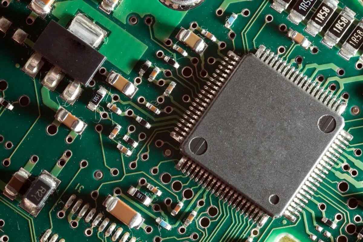
Components of a PCB
A PCB consists of various components that work together to enable the functioning of electronic devices. These components can be broadly categorized into active and passive components.
Active components are those that require a power source to perform their intended functions. These components actively control and manipulate electrical signals. Examples of active components include integrated circuits (ICs), transistors, microcontrollers, and operational amplifiers. These components are responsible for tasks such as signal processing, amplification, and control.
Passive components, on the other hand, do not require an external power source and are used to control the flow of electrical signals. These components include resistors, capacitors, inductors, and diodes. Resistors control the amount of current flowing through a circuit, capacitors store and release electrical energy, inductors store magnetic energy, and diodes allow current to flow in only one direction.
In addition to active and passive components, a PCB may also include other specialized components known as connectors and switches. Connectors allow for the easy connection of external cables and devices to the PCB, while switches provide a means to manually control the flow of electrical signals.
It is important to note that the choice and placement of components on the PCB depend on the specific requirements of the electronic device. Factors such as power consumption, signal integrity, size constraints, and cost considerations must be taken into account during the design process.
Furthermore, proper labeling and documentation of components are essential for effective troubleshooting, repair, and maintenance of the PCB. Each component should be accurately identified using reference designators, which are typically alphanumeric codes, to ensure easy identification and replacement if necessary.
Overall, the proper selection, placement, and integration of components on a PCB are crucial for the successful operation and longevity of electronic devices.
Types of PCBs
Printed Circuit Boards (PCBs) come in various types, each designed to suit specific applications and requirements. The choice of PCB type depends on factors such as complexity, size, functionality, and cost.
1. Single-Sided PCB: This is the simplest and most common type of PCB. It consists of a single layer of substrate material with a thin copper layer on one side. Components are mounted on one side, and the copper traces form the conductive pathways. Single-sided PCBs are cost-effective and widely used in simple electronic devices with minimal circuit complexity.
2. Double-Sided PCB: Double-sided PCBs have a thin copper layer on both sides of the substrate material. Components can be mounted on either side, and the conductive pathways are formed by traces on both sides. Double-sided PCBs offer more flexibility in routing and are commonly used in devices with moderate complexity.
3. Multi-Layer PCB: Multi-layer PCBs consist of three or more layers of substrate material with copper layers sandwiched between them. Each layer is interconnected with vias, which are small holes filled with metal. The additional layers provide more space for components and complex routing, making multi-layer PCBs suitable for high-density and high-performance devices such as smartphones, computers, and network equipment.
4. Rigid PCB: Rigid PCBs are the most common type and are made of rigid materials such as fiberglass or epoxy. They are widely used in various consumer electronics, automotive applications, and industrial equipment. Rigid PCBs offer stability and durability, making them suitable for devices that don’t require flexibility.
5. Flexible PCB: Flexible PCBs, also known as flex PCBs or flex circuits, are made of flexible materials like polyimide. They can be bent, twisted, or folded to fit into tight spaces or conform to unusual shapes. Flexible PCBs are used in applications where space is a constraint or where the device needs to be bent or flexed during use, such as in medical devices, wearables, and aerospace applications.
6. Rigid-Flex PCB: Rigid-flex PCBs combine the advantages of both rigid and flexible PCBs. They consist of a combination of rigid and flexible substrates, interconnected using flexible sections. Rigid-flex PCBs offer the benefits of easy assembly, reduced weight, and improved reliability. They are commonly used in advanced applications such as aerospace, military, and medical devices.
Each type of PCB has its advantages and limitations, and the choice depends on the specific requirements of the electronic device. Designers must consider factors such as cost, complexity, space constraints, durability, and flexibility when selecting the appropriate PCB type.
PCB Manufacturing Process
The manufacturing of a Printed Circuit Board (PCB) involves several stages, each essential for creating a functional and reliable PCB. While specific processes may vary, the general steps involved in PCB manufacturing are as follows:
1. Designing the PCB: The process begins with designing the PCB layout using specialized software. Designers create the schematic, determine the component placement, and define the routing of the traces.
2. Creating the Gerber Files: Once the design is complete, the files in Gerber format are generated. These files contain the information necessary for manufacturing, such as the dimensions, copper layers, solder masks, and silk screens.
3. Making the Substrate: The first step in manufacturing the PCB is creating the substrate, also known as the PCB base or board. The substrate material, usually fiberglass or epoxy, is cut into the desired size and shape.
4. Applying Copper Layers: Copper foil is bonded to the substrate using heat and pressure. The copper foil adheres to the substrate, forming the conductive paths and traces on the PCB.
5. Etching: A chemical etching process is used to remove unwanted copper from the board, leaving only the copper traces as per the design. The etching solution dissolves the exposed copper, creating the required pathways between components.
6. Drilling Holes: Holes are drilled in the PCB to accommodate the through-hole components and provide electrical connections between different layers. Precision drilling machines are used to ensure accurate hole placement.
7. Plating the Holes: To ensure a strong electrical connection, the drilled holes are plated with a thin layer of conductive material, such as copper or tin. This process is known as hole plating or electroplating.
8. Applying Solder Mask: A solder mask layer is applied to the PCB, except for the areas where the solder joints need to be made. The solder mask protects the board from environmental factors and prevents solder bridges between traces during the assembly process.
9. Silk Screening: The final step is applying silk screen printing on the PCB’s surface. This includes adding labels, text, and symbols to indicate component placement, reference designators, and other vital information.
After the manufacturing process is complete, the PCB undergoes testing and quality control procedures to ensure its functionality and reliability. Automated optical inspection (AOI) and electrical testing are commonly performed to detect any defects or issues that need to be addressed before the PCB is used in electronic devices.
How to Design a PCB
Designing a Printed Circuit Board (PCB) requires a systematic approach to ensure functionality, reliability, and manufacturability. Here are the essential steps involved in designing a PCB:
1. Define the Design Requirements: Clearly understand the requirements of the PCB, including the purpose, size constraints, power requirements, and the components that will be mounted on the board.
2. Create a Schematic Diagram: Develop a schematic diagram that represents the circuit connections and components. Use specialized software for schematic capture to accurately document the design.
3. Select the PCB Design Software: Choose a PCB design software that suits your needs and proficiency level. Popular software includes Altium Designer, Eagle, and KiCad. Learn to use the software thoroughly to utilize its full potential.
4. PCB Component Placement: Place the components on the board according to the schematic diagram. Consider factors such as signal flow, thermal management, and accessibility for assembly and maintenance.
5. Route Traces: Establish connections between the components by routing traces on the PCB. Consider signal integrity, power distribution, and noise reduction techniques while routing the traces. Follow design rules and guidelines to ensure proper clearance, trace widths, and impedances.
6. Add Ground and Power Planes: Incorporate ground and power planes in your PCB design to improve signal integrity, minimize noise, and distribute power efficiently. These planes provide stable reference potentials for the circuitry.
7. Perform Design Rule Checking: Utilize the design rule checking (DRC) feature of your PCB design software to identify any design errors and rule violations. Validate that the design meets the manufacturing and assembly specifications.
8. Generate Output Files: Generate the necessary output files, including Gerber files, Drill files, and Assembly Drawings. These files contain the information required for manufacturing and assembly processes.
9. Prototype and Test: Before mass production, it is essential to create a prototype of the PCB and test its functionality. Identify any issues or improvements that need to be addressed.
10. Design Optimization: Refine and optimize the PCB design based on the feedback from prototype testing. Make necessary adjustments to improve performance, reliability, and manufacturability.
11. Documentation: Create comprehensive and accurate documentation that includes the schematic, Bill of Materials (BOM), assembly instructions, test procedures, and any other relevant information. This documentation is essential for future reference, troubleshooting, and maintenance.
By following these steps and continuously improving your PCB designing skills, you can create functional and efficient PCB designs that meet the requirements of your electronic projects.
Important Considerations in PCB Design
Designing a Printed Circuit Board (PCB) requires careful consideration of various factors to ensure the functionality, reliability, and manufacturability of the final product. Here are some important considerations to keep in mind during the PCB design process:
1. Component Placement: Proper component placement is crucial for efficient circuit operation. Place components strategically to optimize signal flow, minimize noise, and facilitate effective thermal management. Consider components that require higher power and place them away from sensitive components.
2. Signal Integrity: Pay attention to signal integrity to ensure that signals travel accurately without distortion or degradation. Consider impedance control, trace length matching, and minimizing signal reflections. Proper grounding and shielding techniques can also help maintain signal integrity.
3. Power Distribution: Plan and optimize the power distribution network on the PCB to ensure stable and adequate power supply to all components. Use power planes or dedicated power traces to minimize voltage drops and ensure efficient power delivery.
4. Thermal Management: Electronic components generate heat, which can impact their performance and reliability. Consider thermal management techniques such as adding heat sinks, thermal vias, and proper ventilation to dissipate heat effectively and prevent overheating.
5. Design for Manufacturability (DFM): Design the PCB with manufacturing in mind. Consider the capabilities of the manufacturing process, such as minimum trace widths, minimum drill sizes, and other design rules. Simplify the design to reduce manufacturing complexities and costs.
6. Design for Assembly (DFA): Optimize the PCB design for ease of assembly. Consider the order of component placement, access for soldering or inspection, and the use of surface mount components versus through-hole components. Minimize the need for manual assembly and reduce the chance of assembly errors.
7. EMI/EMC Considerations: Electromagnetic Interference (EMI) and Electromagnetic Compatibility (EMC) are vital considerations. Implement proper grounding techniques, shielding measures, and separate sensitive components from noisy components to minimize EMI and ensure compliance with EMC regulations.
8. Testability: Design the PCB with testability in mind. Incorporate test points, such as via pads or dedicated test pads, to facilitate testing and debugging procedures. This enables easier troubleshooting and reduces the time required for fault identification and rectification.
9. Environmental Considerations: Consider the intended environment in which the PCB will be used. Design for adequate protection against moisture, vibration, temperature, and other environmental factors that may affect the performance and reliability of the PCB.
10. Documentation and Communication: Maintain detailed and accurate documentation throughout the design process. This includes the schematic diagram, PCB layout files, and the Bill of Materials (BOM). Effective communication with manufacturers, assemblers, and other stakeholders is essential for successful PCB production.
By considering these important factors, you can enhance the functionality, reliability, and manufacturability of your PCB designs, resulting in successful electronic devices.
Common PCB Issues and Troubleshooting Tips
While PCB design and manufacturing processes have become more advanced, issues can still arise that affect the functionality and performance of the board. Here are some common PCB issues and troubleshooting tips:
1. Short Circuits: Short circuits occur when two or more conductive paths unintentionally connect. A common cause is a solder bridge between adjacent traces or pins. Inspect the PCB for any visible bridges and use a multimeter to identify the short circuit. Use solder wick or desoldering braid to remove excess solder and separate the conductive paths.
2. Open Circuits: Open circuits happen when there is a break or disconnection in a conductive path. This can be caused by a faulty solder joint, broken trace, or a component not properly connected. Use a multimeter to identify the open circuit and visually inspect the affected area for any visible damage. Repair the open circuit by reflowing the solder or repairing the broken trace using wire or copper tape.
3. Component Placement Errors: Incorrectly placed components can lead to functional or electrical issues. Verify the component values and their orientations against the schematic and ensure they are placed correctly on the PCB. If a component is misplaced, carefully desolder it and reposition it in the correct location.
4. Power and Ground Issues: Inadequate power and ground connections can cause erratic behavior, noise, or failure of the PCB. Check the continuity of power and ground traces using a multimeter. Ensure proper grounding techniques, such as connecting the ground plane to all components and minimizing trace length for power connections.
5. Noise and Signal Integrity Problems: Noise interference can disrupt the proper functioning of a PCB, leading to signal integrity issues. Use proper grounding and shielding techniques, minimize the length of high-speed signal traces, and ensure proper filtering and decoupling of power lines. Consider using controlled impedance traces to maintain signal integrity.
6. Overheating and Thermal Issues: Inadequate thermal management can lead to component overheating and failure. Ensure proper ventilation, use heat sinks or thermal vias to dissipate heat, and optimize component placement to avoid heat concentration. Monitor component temperatures and consider using thermal analysis tools to identify potential hotspots.
7. Manufacturing Defects: PCBs can sometimes have manufacturing defects, including incorrect drill holes, misaligned layers, or solder mask errors. Perform a visual inspection of the PCB for such defects and contact the manufacturer for proper resolution or replacement.
8. ESD Damage: Electrostatic discharge (ESD) can cause damage to sensitive components. Take proper precautions such as using an ESD wrist strap, anti-static mat, and proper handling techniques to prevent ESD damage during assembly, testing, and handling of the PCB.
9. Test and Debugging Procedures: Having a well-defined test and debugging process can help identify and resolve PCB issues effectively. Develop test procedures and use appropriate testing equipment, such as a multimeter, oscilloscope, or logic analyzer, to troubleshoot and diagnose problems.
10. Consultation and Support: If you encounter complex or persistent issues with your PCB, consider seeking consultation and support from experienced PCB designers, manufacturers, or online forums. They may provide valuable insights, recommendations, or solutions to address the specific issue at hand.
By being aware of these common PCB issues and implementing proper troubleshooting techniques, you can identify and resolve problems effectively, ensuring the functionality and reliability of your PCB designs.
Advantages and Limitations of PCBs
Printed Circuit Boards (PCBs) offer numerous advantages in terms of functionality, reliability, and cost-effectiveness. However, they also have certain limitations that need to be considered. Let’s explore the advantages and limitations of PCBs:
Advantages of PCBs:
1. Compact and Space-Efficient: PCBs allow for a high density of components and interconnections in a compact space. This makes them ideal for devices where size is a constraint, such as smartphones, laptops, and wearables.
2. High Reliability: PCBs provide a reliable platform for electronic components, ensuring secure connections and consistent performance. The use of standardized production techniques and quality control measures contributes to the overall reliability of PCB-based systems.
3. Ease of Mass Production: PCBs can be efficiently manufactured in large quantities through automated processes, making them cost-effective for mass production. This enables electronic devices to be produced at a lower cost, making them accessible to a wider market.
4. Design Flexibility: PCB designs are highly flexible and customizable. Components can be easily integrated and interconnected according to specific design requirements, allowing for optimum functionality and performance.
5. Signal Integrity: PCB designs can incorporate techniques such as controlled impedance traces, ground planes, and signal routing optimization to maintain signal integrity. This ensures proper signal transmission and reduces the risk of noise or interference.
Limitations of PCBs:
1. Complexity Limitations: PCBs may have limitations in terms of complexity due to size constraints or manufacturing capabilities. Highly complex circuits or devices may require multi-layer PCBs or alternative technologies to accommodate the required complexity.
2. Design Modifications: Once a PCB design is produced, making changes or modifications to the design can be challenging and costly. This limitation underscores the importance of thorough design planning and validation before production.
3. Environmental Impact: PCBs contain materials that may pose environmental challenges if not disposed of properly. Some components, like lead-based solder, have raised environmental concerns, necessitating compliance with regulations for their safe handling and disposal.
4. Costly Prototyping: The initial prototyping phase of PCB development can be costly, especially for small-scale production or when design modifications are required. Prototyping expenses include materials, equipment, and labor costs.
5. Limited Flexibility: While flexible PCBs are available, traditional rigid PCBs lack the flexibility of other electronic interconnect methods. Applications requiring extreme flexibility or bending may not be suitable for rigid PCBs.
Despite these limitations, the advantages of PCBs far outweigh their drawbacks. Their reliability, cost-effectiveness, and design flexibility make PCBs the preferred choice for a wide range of electronic devices.
Future Trends in PCB Technology
As technology advances at a rapid pace, the field of Printed Circuit Board (PCB) technology continues to evolve and innovate. Here are some future trends that are expected to shape the PCB industry:
1. Miniaturization and High-Density Interconnections: A significant trend in PCB technology is the continuous drive towards miniaturization and high-density interconnections. As electronic devices become smaller and more powerful, PCBs need to accommodate a higher number of components and interconnections within limited space. This requires advanced manufacturing processes and the development of finer trace widths, smaller vias, and microscopic components.
2. Flexible and Stretchable PCBs: The demand for flexible electronics is growing rapidly, leading to advancements in flexible and stretchable PCB technology. Flexible PCBs, or flex PCBs, are ideal for applications requiring bendability, such as wearables, medical devices, and curved displays. Future trends in this area include the development of new materials and techniques to enhance the flexibility, durability, and reliability of these PCBs.
3. Integrated Passive Devices (IPDs): Integrated Passive Devices are a growing trend in PCB technology. IPDs combine passive components, such as resistors, capacitors, and inductors, directly on the PCB, reducing the need for separate discrete components. This integration of passive components can further enhance miniaturization, improve signal integrity, and reduce the overall cost and complexity of PCB designs.
4. High-Frequency PCBs: With the increasing demand for high-speed data transfer and wireless communication, there is a rising need for high-frequency PCBs. These PCBs are designed to handle signals in the gigahertz (GHz) range, ensuring minimal signal loss and interference. Advancements in materials, stack-up designs, and signal integrity analysis tools are driving the development of high-frequency PCBs.
5. Advanced Materials: The use of advanced materials in PCB manufacturing is a key trend. New materials with improved electrical properties, thermal conductivity, and mechanical strength are being introduced to address the challenges posed by high-speed applications and miniaturization. Examples include low-loss dielectric materials, conductive polymers, and metal matrix composites.
6. 3D-Printed PCBs: Additive manufacturing techniques, such as 3D printing, are making their way into PCB production. 3D-printed PCBs offer design flexibility, rapid prototyping capabilities, and the possibility of creating complex geometries that would be challenging with traditional manufacturing methods. This trend has the potential to revolutionize the PCB industry by enabling faster design iterations and customization.
7. Increased Automation and AI-Based Design: Automation and artificial intelligence (AI) are expected to play a significant role in future PCB design and manufacturing processes. AI algorithms can aid in optimizing PCB layouts, ensuring better signal integrity, and detecting potential design errors. The use of automation, robotics, and machine learning can also streamline assembly processes and improve overall efficiency.
These future trends in PCB technology signify the continuous efforts to push the boundaries of performance, functionality, and manufacturing capabilities. As the demand for smaller, more powerful, and flexible electronic devices grows, PCB technology will continue to evolve to meet these evolving needs.