
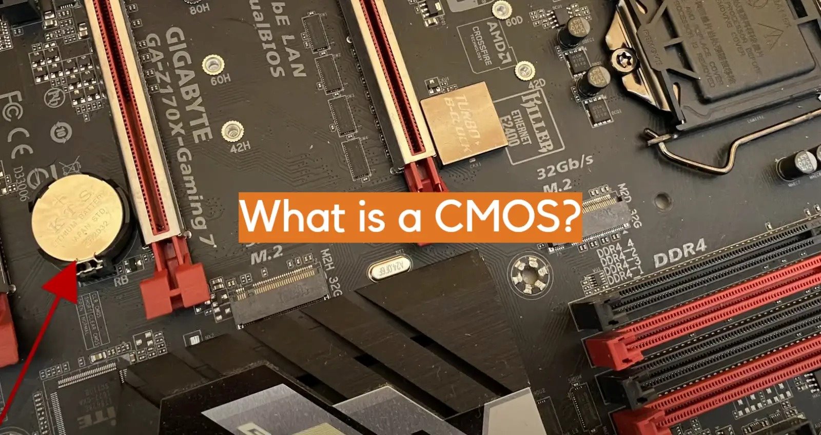
What is CMOS?
CMOS, which stands for Complementary Metal-Oxide-Semiconductor, is a type of semiconductor technology that is widely used in the manufacturing of electronic devices. It is a key technology in the field of integrated circuits, allowing for the miniaturization and integration of complex electronic components into a single chip. CMOS technology has revolutionized the electronics industry and has become the backbone of modern digital devices.
At its core, CMOS is a combination of two types of transistors: P-type (positive) and N-type (negative) transistors. These transistors are paired together to form a complementary pair, hence the name “complementary” in CMOS. The key feature of CMOS is its low power consumption, making it extremely energy-efficient compared to other technologies.
CMOS technology is widely used in a variety of electronic devices we use on a daily basis. For instance, it is the underlying technology behind processors in computers, smartphones, tablets, and other digital devices. It is also used in memory chips, image sensors, and other integrated circuits.
The way CMOS technology works is by using a combination of different voltages to control the flow of electric current through the transistors. When an electrical signal is applied, the transistors either allow or block the current flow, thereby creating the binary logic required for digital electronics.
One of the key advantages of CMOS technology is its low power consumption. Unlike other semiconductor technologies, CMOS only consumes power when it is required to perform a specific task. This makes it ideal for battery-powered devices where energy efficiency is crucial. Additionally, CMOS circuits produce less heat, leading to improved reliability and longer lifespan of the devices.
Furthermore, CMOS technology offers excellent noise immunity, allowing for reliable signal transmission even in the presence of electromagnetic interference. This makes CMOS ideal for applications that require high-speed data processing and transmission, such as in communication systems and networking devices.
Understanding CMOS Technology
CMOS technology is based on the use of metal-oxide-semiconductor field-effect transistors (MOSFETs), which are the building blocks of integrated circuits. MOSFETs are tiny electronic switches that control the flow of electrical current. In CMOS technology, these MOSFETs are arranged in a complementary pair, consisting of a P-type and an N-type transistor.
The P-type transistor is made of a semiconductor material doped with impurities that create an excess of positive charge carriers, known as holes. On the other hand, the N-type transistor is made of a semiconductor material doped with impurities that create an excess of negative charge carriers, known as electrons. It is the combination of these two types of transistors that gives CMOS its complementary nature.
CMOS technology operates on binary logic, where information is represented in terms of binary digits or bits – either 0 or 1. It uses voltage levels to represent these binary states. For example, a low voltage level might represent a logic 0, while a high voltage level might represent a logic 1.
One of the key features of CMOS technology is its ability to retain the state of a gate (a combination of transistors) when no power is applied. This is achieved through the use of a capacitor to store the charge that represents the logic state. As a result, CMOS circuits consume power primarily during switching and require little to no power when the circuit remains static.
Another important aspect of CMOS technology is its scalability. Over the years, CMOS technology has been continuously scaled down to smaller feature sizes, allowing more transistors to be packed onto a single chip. This has led to the development of highly complex and powerful integrated circuits that can perform intricate tasks with remarkable speed and efficiency.
Furthermore, CMOS technology offers the advantage of high noise immunity. The complementary nature of the transistors allows for better noise rejection, ensuring that the desired signals are preserved even in the presence of interference. This makes CMOS technology highly reliable, especially in applications that demand high signal integrity.
How does CMOS work?
CMOS technology operates by using switches known as MOSFETs, or metal-oxide-semiconductor field-effect transistors. These transistors are incredibly tiny and can be fabricated onto a silicon wafer, forming the basis of integrated circuits.
Each MOSFET consists of three main parts: the source, the drain, and the gate. The source and drain are connected by a conductive channel that controls the flow of electrical current. The gate, which is made of a thin layer of insulating material, is placed in between the source and drain and acts as a control mechanism.
The MOSFETs used in CMOS technology can be classified into two types: P-type and N-type transistors. The P-type transistor is created by doping the silicon with impurities that introduce positive charge carriers, or holes. The N-type transistor, on the other hand, is created by doping the silicon with impurities that introduce negative charge carriers, or electrons.
When a voltage is applied to the gate of the MOSFET, it creates an electric field that controls the flow of charge carriers through the channel. The MOSFET can be in either an “on” state or an “off” state, depending on the voltage applied to the gate.
In the “off” state, the transistor acts as an open switch, blocking the flow of current between the source and drain. This occurs when the voltage applied to the gate is insufficient to overcome the threshold voltage of the transistor. As a result, the channel remains non-conductive, and no current flows.
In the “on” state, the transistor acts as a closed switch, allowing current to flow between the source and drain. This occurs when the voltage applied to the gate exceeds the threshold voltage of the transistor. The electric field created by the gate voltage attracts charge carriers (either holes or electrons) to form a conductive channel between the source and drain, enabling the flow of current.
The use of complementary P-type and N-type transistors is the key to CMOS technology’s efficiency and low power consumption. This complementary nature allows for the creation of complex circuits capable of performing logic operations, such as AND, OR, and NOT functions.
CMOS circuits are designed using a combination of these logic gates to perform the desired functions. By arranging and connecting the MOSFETs in different ways, CMOS technology can realize complex digital circuitry that powers a wide range of electronic devices we use today.
The Advantages of CMOS
CMOS technology offers a wide range of advantages that have made it the preferred choice for the fabrication of integrated circuits. From its low power consumption to its scalability, CMOS technology excels in many aspects.
One of the key advantages of CMOS is its low power consumption. Compared to other semiconductor technologies, CMOS circuits consume significantly less power. This is due to the fact that CMOS devices only draw power when they are actively switching, resulting in reduced energy requirements and longer battery life in portable devices.
Additionally, CMOS circuits produce less heat compared to other technologies. The low power consumption of CMOS means that less energy is wasted in the form of heat, leading to improved device reliability and reduced thermal management requirements. This is particularly important for applications where heat dissipation is a concern, such as high-performance computing systems.
Another advantage of CMOS technology is its excellent noise immunity. The complementary nature of CMOS circuits allows for better noise rejection, ensuring that the desired signals are preserved even in the presence of electromagnetic interference. This makes CMOS technology highly reliable in applications that require high signal integrity, such as communication systems and medical devices.
CMOS technology also offers great flexibility when it comes to fabrication. It allows for the integration of numerous complex functions onto a single chip, reducing the physical size and weight of electronic devices. Furthermore, CMOS technology is highly scalable, meaning that it can be continuously improved and miniaturized to accommodate increasingly smaller feature sizes. This scalability enables the development of more powerful and efficient electronic components.
Moreover, CMOS technology enables the integration of digital and analog components on the same chip. This allows for the seamless combination of digital processing and analog signal conditioning, which is essential in many applications, including audio amplifiers, data converters, and sensor interfaces.
Cost-effectiveness is another advantage of CMOS technology. Over the years, CMOS has become a widely adopted and mature technology, resulting in economies of scale in manufacturing. This has led to reduced production costs, making CMOS technology more accessible and affordable for a wide range of applications.
Overall, the advantages of CMOS technology, including low power consumption, scalability, noise immunity, flexibility, integration capabilities, and cost-effectiveness, have contributed to its prominence in the electronics industry. As technology continues to advance, CMOS is expected to play a vital role in the development of innovative and efficient electronic devices.
Applications of CMOS Technology
CMOS technology finds diverse applications across various industries, thanks to its versatility and efficient performance. Let’s explore some of the key areas where CMOS technology plays a vital role.
One of the primary applications of CMOS technology is in the manufacturing of microprocessors and central processing units (CPUs) for computers and smartphones. The low power consumption and high-speed capabilities of CMOS make it an ideal choice for these computing devices, enabling efficient data processing and multitasking.
CMOS technology is also widely used in memory devices, such as RAM (Random Access Memory) and flash memory. The scalability of CMOS allows for the integration of a large number of memory cells, enabling higher storage capacities and faster data access.
In the field of imaging, CMOS image sensors have replaced traditional CCD (Charge-Coupled Device) sensors in many applications. CMOS image sensors offer lower power consumption and higher integration capabilities, making them suitable for digital cameras, smartphones, surveillance systems, and medical imaging devices.
Furthermore, CMOS technology plays a crucial role in communication systems. It is used in the fabrication of radio frequency (RF) integrated circuits for wireless transceivers, allowing for efficient signal processing, modulation, and demodulation. CMOS technology also enables the development of high-speed data converters and communication interfaces.
The automotive industry heavily relies on CMOS technology for various applications. It is used in advanced driver assistance systems (ADAS), such as collision detection, lane departure warning, and adaptive cruise control. CMOS technology is also integrated into entertainment systems, navigation systems, and vehicle diagnostics.
CMOS technology has made significant contributions to the healthcare sector as well. It is used in medical imaging equipment, such as X-ray detectors, ultrasound transducers, and digital mammography systems. CMOS biosensors are utilized for DNA analysis, protein detection, and point-of-care diagnostics, enabling faster and more accurate diagnosis of diseases.
Other notable applications of CMOS technology include consumer electronics like digital cameras, gaming consoles, and wearable devices. It is also used in industrial automation, robotics, aerospace, defense systems, and energy management systems.
The versatility and efficiency of CMOS technology make it an indispensable part of many cutting-edge technologies. With continued advancements and innovations, we can expect to see CMOS technology being integrated into even more applications in the future, further transforming the way we live, work, and communicate.
CMOS vs. Other Technologies
CMOS technology is not the only semiconductor technology available in the market. It competes with other technologies, such as Bipolar Junction Transistor (BJT) and Field-Effect Transistor (FET), each with their own strengths and weaknesses. Let’s compare CMOS with these technologies to understand their differences.
One of the key advantages of CMOS technology is its low power consumption. CMOS circuits consume minimal power when in a static state, making them ideal for energy-efficient applications. In contrast, BJT technology consumes power continuously, even when the device is not actively switching. This makes CMOS more suitable for battery-powered devices and systems that require longer battery life.
Another advantage of CMOS is its scalability. CMOS technology can be easily scaled down to smaller feature sizes, enabling the integration of more transistors on a single chip. This allows for higher performance and increased functionality. BJT technology, on the other hand, faces limitations in scaling due to its inherent design characteristics, making it less suitable for highly integrated circuits.
CMOS technology also offers superior noise immunity compared to BJT. The complementary nature of CMOS transistors provides better noise rejection, ensuring reliable signal transmission in the presence of electromagnetic interference. BJT technology, although renowned for its high-speed capabilities, is more susceptible to noise, making it less suitable for applications that require high signal integrity.
When comparing CMOS with FET technology, the primary difference lies in the gate structure of the transistors. CMOS employs metal-oxide-semiconductor (MOS) transistors, while FET technology encompasses various types, such as MOSFETs and JFETs (Junction Field-Effect Transistors). While CMOS is renowned for its low power consumption, FETs offer advantages in terms of high input impedance and low noise. FETs are often used in high-frequency applications, where low noise and signal amplification are critical.
Additionally, CMOS technology has the attribute of mixed-signal integration, enabling the combination of digital and analog circuitry on a single chip. This makes CMOS suitable for applications that require both digital processing and analog signal conditioning. BJT and FET technologies, on the other hand, tend to focus more on either digital or analog functionality.
Challenges and Limitations of CMOS
While CMOS technology offers numerous advantages, it also faces certain challenges and limitations that need to be addressed for its continued improvement and usage. Let’s explore some of these challenges.
One significant challenge is the issue of power leakage. Although CMOS technology is renowned for its low power consumption, it still faces concerns related to power leakage when the circuit is in a standby or idle state. This power leakage can lead to unnecessary energy consumption and reduced overall efficiency. Efforts have been made to reduce power leakage through advanced design techniques and the development of low-leakage process technologies.
The ongoing miniaturization of CMOS transistors poses another challenge. As feature sizes continue to shrink, new issues arise, such as increased transistor variability, higher susceptibility to process variations, and greater sensitivity to environmental factors. These challenges can impact the performance and reliability of CMOS devices, and addressing them requires continuous research and innovation in process technologies and fabrication techniques.
One limitation of CMOS technology is the speed constraints imposed by its low-voltage operation. CMOS performance is directly linked to the supply voltage, and reducing the voltage to achieve low power consumption can result in decreased speed. While efforts have been made to improve CMOS speed through low-power design methodologies, there are inherent trade-offs between power consumption and performance.
Another limitation of CMOS technology is its vulnerability to radiation-induced errors. High-energy particles, such as cosmic ray neutrons, can cause transient faults in CMOS circuits, leading to errors in the computation or storage of data. This can be a critical issue in applications that require high reliability and fault-tolerance, such as in aerospace or nuclear systems. Techniques like radiation-hardened design and error-detection and correction mechanisms are employed to mitigate the impact of radiation-induced errors.
Manufacturing complexity and cost represent additional challenges for CMOS technology. As feature sizes become smaller, the fabrication process becomes more intricate, requiring advanced lithography techniques and expensive equipment. This can make the production of CMOS devices costly, especially for smaller-scale manufacturers or niche applications. However, economies of scale, improved manufacturing techniques, and industry advancements have helped address these challenges to a certain extent.
Despite these challenges and limitations, CMOS technology continues to be the dominant choice for integrated circuit manufacturing due to its versatility, low power consumption, scalability, and cost-effectiveness. Researchers and engineers are actively working on addressing these challenges through innovations in design, process technology, and circuit optimization, paving the way for further improvements in CMOS technology.
Future Developments in CMOS Technology
CMOS technology has undergone significant advancements over the years, but the innovation doesn’t stop there. Researchers and engineers are continuously working on pushing the boundaries of CMOS technology to meet the evolving demands of the digital age. Let’s explore some of the exciting future developments in CMOS technology.
One area of focus is the continued scaling of CMOS transistors. As feature sizes shrink, researchers are exploring alternative materials and transistor structures to overcome the limitations posed by traditional CMOS. This includes the investigation of new channel materials, such as III-V semiconductors, and the development of novel transistor architectures, like nanowire transistors and tunnel field-effect transistors (TFETs). These advancements aim to further improve device performance, reduce power consumption, and enable higher integration densities.
Another direction of CMOS technology development is the exploration of new system architectures, such as neuromorphic computing and quantum computing. Neuromorphic computing aims to replicate the functionality of the human brain by integrating neural networks directly into CMOS circuits. Quantum computing, on the other hand, explores the use of quantum bits (qubits) to perform complex calculations. The development of CMOS-compatible qubits and circuitry is crucial for enabling practical quantum computing systems.
Improvements in packaging and interconnect technologies are also anticipated. As the integration of more transistors on a single chip increases, there is a need for advanced packaging techniques that allow for efficient heat dissipation, signal transmission, and power delivery. This includes the exploration of new materials, 3D stacking technologies, and innovative interconnect architectures to further enhance the performance and reliability of CMOS devices.
Energy efficiency remains a significant focus for future CMOS developments. Researchers are exploring new circuit and architecture designs, such as near-threshold computing and adaptive power management techniques, to maximize energy efficiency without compromising performance. This will be particularly essential for the proliferation of battery-powered devices and the growth of Internet of Things (IoT) applications.
The emergence of new fabrication technologies, such as extreme ultraviolet (EUV) lithography and directed self-assembly, holds promise for overcoming the challenges of scaling CMOS beyond current limits. These technologies offer higher resolution and improved manufacturing processes that can enable the production of even smaller and more complex CMOS devices. Advancements in materials science, including the development of new dielectric materials and high-mobility channel materials, will further contribute to the future of CMOS technology.
Furthermore, advancements in artificial intelligence (AI) and machine learning are expected to have a significant impact on CMOS technology. The integration of AI-specific accelerators, such as neuromorphic and tensor processing units, into CMOS circuits will enable more efficient and intelligent data processing in various applications, including robotics, autonomous vehicles, and personalized computing devices.
Overall, the future of CMOS technology is poised for exciting developments. From scaling to new materials, from novel architectures to advanced packaging, researchers and engineers are constantly innovating to unleash the full potential of CMOS. These advancements will shape the next generation of electronic devices, revolutionizing industries and transforming the way we live, work, and connect.