
What Does BGA Stand For?
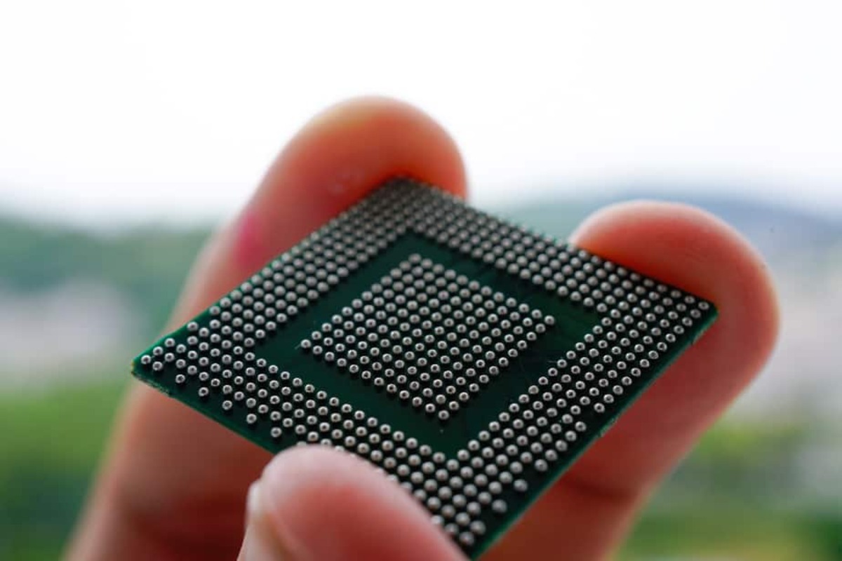
When it comes to the world of electronics, the acronym BGA stands for Ball Grid Array. It is a packaging technology used in electronic components that has gained popularity due to its numerous advantages over traditional packaging methods.
In a BGA, the electronic component is mounted onto a small substrate, which is typically a printed circuit board (PCB). The component is then connected to the PCB using an array of tiny spherical balls made of solder. These solder balls act as the electrical and mechanical connection between the component and the PCB, allowing for efficient and reliable performance.
One of the key advantages of BGA technology is its high level of integration. BGA packages allow for a larger number of connections compared to other packaging methods, such as through-hole components. This density of connections enables BGA packages to support complex electronic circuitry, making them suitable for applications that require high-performance computing and data processing.
Furthermore, BGA packages offer excellent thermal conductivity. The solder balls provide a direct path for heat dissipation, allowing for efficient cooling of the electronic component. This makes BGA packages well-suited for devices that generate a significant amount of heat, such as microprocessors and graphic processing units (GPUs).
Another advantage of BGA technology is its improved signal integrity. The shorter electrical paths between the component and the PCB, as well as the reduced parasitic capacitance and inductance, result in faster and more reliable signal transmission. This makes BGA packages highly desirable for applications that require high-speed and low noise operation, such as telecommunications and consumer electronics.
BGA packages also offer better mechanical stability compared to through-hole components. The solder balls provide a strong and secure connection, reducing the risk of damage due to mechanical stresses, vibrations, and shocks. This enhanced durability makes BGA packages suitable for harsh environments and applications that require long-term reliability.
Advantages of BGA Technology
The use of Ball Grid Array (BGA) technology in electronic components provides several advantages over traditional packaging methods. These advantages contribute to improved performance, enhanced reliability, and greater design flexibility. Here are some key advantages of BGA technology:
- Higher Integration: BGA packages allow for a higher number of connections compared to through-hole components. This enables more complex electronic circuitry, making BGA packages suitable for high-performance applications.
- Improved Thermal Conductivity: BGA packages have excellent thermal conductivity due to the direct contact between the component and the PCB through solder balls. This efficient heat dissipation makes BGA packages ideal for devices that generate substantial heat.
- Better Signal Integrity: With shorter electrical paths and reduced parasitic capacitance and inductance, BGA packages offer improved signal integrity. This is crucial for high-speed and low noise operation in applications like telecommunications and consumer electronics.
- Enhanced Mechanical Stability: The solder balls in BGA packages provide a strong and secure connection, making them highly resistant to mechanical stresses, vibrations, and shocks. This increased mechanical stability ensures long-term reliability in harsh environments.
- Smaller Size: BGA packages are generally smaller in size compared to through-hole components. This compact form factor allows for greater design flexibility and more efficient use of space on the PCB.
- Cost-Effective Production: BGA packages can be assembled using automated equipment, reducing production costs. The high level of integration and efficient use of space also contribute to cost savings in terms of material usage and PCB size.
Overall, BGA technology offers numerous advantages that make it a preferred choice in many electronic applications. The higher integration, improved thermal conductivity, better signal integrity, enhanced mechanical stability, smaller size, and cost-effective production make BGA packages a reliable and efficient packaging solution for a wide range of electronic components.
How Does BGA Work?
Ball Grid Array (BGA) technology works by using an array of tiny spherical balls made of solder to connect electronic components to a printed circuit board (PCB). The BGA package consists of a substrate that serves as the foundation for mounting the component and a series of solder balls that establish electrical and mechanical connections.
The BGA package is first attached to the PCB by aligning the solder balls with corresponding pads on the PCB. The component is then heated to a temperature that melts the solder balls, allowing them to bond with the PCB. As the solder cools and solidifies, it creates a secure and reliable connection between the component and the PCB.
The number and arrangement of the solder balls on a BGA package vary depending on the specific component and the desired level of integration. Smaller components may have a few dozen solder balls, while larger ones can have hundreds or even thousands of balls.
The solder balls not only establish the electrical connection between the component and the PCB but also provide mechanical support. They form a sturdy interface that can withstand mechanical stresses, vibrations, and shocks, ensuring the stability and reliability of the electronic assembly.
During operation, the BGA package facilitates the transfer of electrical signals between the component and the PCB through the solder balls. These balls act as conductive pathways, allowing the flow of current and data between the component and other parts of the circuit.
Moreover, the solder balls in a BGA package also play a crucial role in thermal management. They provide a direct path for heat dissipation from the component to the PCB. This efficient cooling mechanism helps prevent overheating and ensures the proper functioning and longevity of the electronic device.
BGA vs. Through-Hole Components
When it comes to electronic packaging, Ball Grid Array (BGA) technology has emerged as a popular alternative to traditional through-hole components. Here, we will compare the two methods and highlight the advantages and disadvantages of each.
Through-hole components are mounted on a PCB by inserting their leads into drilled holes and soldering them to the copper traces on the other side of the board. This method offers simplicity and reliability, making it suitable for applications that require robust mechanical connections and ease of repair.
On the other hand, BGA components utilize an array of tiny spherical balls made of solder to establish both electrical and mechanical connections. This technology offers several advantages over through-hole components, including higher integration, improved thermal performance, and better signal integrity.
In terms of integration, BGA packages allow for a greater number of connections compared to through-hole components. This increased density enables more complex circuitry and miniaturization, making BGA packages ideal for high-performance applications where space is at a premium.
BGA packages also offer superior thermal performance. The solder balls provide a direct pathway for heat dissipation, resulting in efficient cooling. In contrast, through-hole components rely on the PCB traces to transfer heat, which may not be as effective, especially for components that generate substantial heat.
When it comes to signal integrity, BGA packages have the advantage of shorter electrical paths, reduced parasitic capacitance, and inductance. This leads to faster and more reliable signal transmission, making BGA technology suitable for high-speed and low noise applications like telecommunications and consumer electronics.
While BGA components offer these advantages, they do come with some challenges. First, BGA packages are more difficult to repair or replace compared to through-hole components. Their complex nature and the need for specialized equipment make rework and repair a cumbersome process.
Furthermore, through-hole components have the advantage of being more forgiving in terms of assembly and PCB design tolerances. BGA packages require precise alignment and soldering techniques, making their assembly more critical and potentially prone to manufacturing issues.
In short, BGA technology outshines through-hole components in terms of integration, thermal performance, and signal integrity. However, the challenges in repair and assembly must be considered when selecting the appropriate packaging method for a specific application.
Types of BGA Packages
Ball Grid Array (BGA) packages come in various types, each designed to meet specific requirements in terms of size, pin count, and electrical performance. Here are some commonly used types of BGA packages:
- Plastic Ball Grid Array (PBGA): PBGA packages are the most common type of BGA packages. They have a plastic substrate that provides insulation and mechanical support for the component. PBGA packages are available in a wide range of pin counts and sizes, making them suitable for many applications.
- Ceramic Ball Grid Array (CBGA): CBGA packages use a ceramic substrate instead of plastic. Ceramic offers better thermal conductivity and mechanical stability, making CBGA packages well-suited for applications that require high reliability and efficient thermal management.
- Micro Ball Grid Array (µBGA): µBGA packages are characterized by their smaller size and finer pitch compared to standard BGA packages. They are often used in mobile devices, where space is limited. The reduced size and pitch of µBGA packages allow for greater circuit density and miniaturization.
- Flip Chip Ball Grid Array (FCBGA): FCBGA packages use flip chip technology, where the component is mounted face down to create a direct electrical connection between the die and the substrate. This eliminates the need for wire bonding and provides better thermal and electrical performance.
- Quad Flat No-Lead (QFN): Although not technically a BGA package, QFN packages feature a similar solder ball grid array construction. The main difference is the absence of a substrate; the component is directly mounted on the PCB. QFN packages are known for their small size, excellent thermal performance, and low cost.
Each type of BGA package offers unique advantages and has specific use cases. The choice of the package type depends on factors such as the required pin count, size constraints, thermal considerations, and cost considerations. Designers must carefully evaluate these factors to select the most appropriate BGA package for their specific application.
BGA and PCB Design Considerations
When incorporating Ball Grid Array (BGA) packages into printed circuit board (PCB) designs, several considerations must be taken into account. Proper PCB design is crucial for ensuring the successful integration and reliable performance of BGA components. Here are some key design considerations:
- Pad and Solder Mask Design: The layout of solder pads on the PCB is critical for proper connection and soldering of BGA packages. The pad size, shape, and spacing should match the BGA component’s specifications to ensure proper alignment and solder joint formation. Additionally, the application of solder mask should be carefully controlled to prevent solder bridging between adjacent pads.
- Thermal Management: Effective thermal management is essential for maximizing the reliability and performance of BGA components. Proper placement of thermal vias, copper pours, and heatsinks on the PCB can help dissipate heat from the BGA packages. Good thermal design practices should be implemented to prevent excessive heat buildup and ensure adequate cooling.
- Signal Integrity: BGA packages require careful attention to signal integrity to maintain reliable communication between the component and the rest of the circuit. Proper trace routing, controlled impedance, and signal length matching should be considered to minimize signal degradation and electromagnetic interference (EMI).
- Power Delivery: BGA components often require multiple power supply pins to meet their power requirements, especially for high-speed and high-power applications. Adequate power and ground planes should be incorporated into the PCB design to ensure proper power delivery and minimize voltage drops or noise issues.
- BGA Fanout: The fanout design refers to the routing of signals from the BGA package’s solder balls to the rest of the PCB. This can be a complex task due to the high pin count and fine pitch of BGA packages. Careful consideration should be given to the routing density, impedance matching, and signal length matching to maintain signal integrity during the fanout process.
- Assembly and Rework: The BGA package’s assembly and rework process should be considered during PCB design. Adequate spacing, access points, and test points should be provided to enable successful and efficient assembly and rework operations. Additionally, considerations for inspection, testability, and repairability should also be taken into account.
By paying careful attention to these design considerations, PCB designers can ensure a successful integration of BGA packages into electronic systems. Proper pad and solder mask design, thermal management, signal integrity, power delivery, fanout design, and assembly/rework considerations lay the foundation for reliable and efficient operation of BGA components on the PCB.
Factors Affecting BGA Reliability
The reliability of Ball Grid Array (BGA) components is crucial for their successful operation in electronic systems. Several factors can impact the reliability of BGA packages, and understanding these factors is essential for ensuring long-term performance. Here are some key factors affecting BGA reliability:
- Solder Joint Integrity: The integrity of solder joints is critical for the reliability of BGA packages. Factors such as solder alloy composition, component and PCB pad metallization, and soldering process parameters can all impact the strength and durability of the solder joints. Proper control and optimization of these factors are crucial to maintain reliable electrical and mechanical connections.
- Thermal Cycling Stress: BGA packages are often exposed to thermal cycling stress due to temperature variations during operation. This stress can cause fatigue and failure in the solder joints over time. Proper thermal management, including efficient heat dissipation, thermal expansion matching, and avoiding excessive temperature changes, can help mitigate the effects of thermal cycling stress.
- Thermal and Mechanical Mismatch: BGA packages experience different coefficients of thermal expansion (CTEs) between the component, substrate, and PCB. This thermal and mechanical mismatch can lead to stress accumulation, which can potentially damage the solder joints or the component itself. Good design practices, including appropriate substrate and PCB material selection, thermal vias, and controlled impedance structures, can mitigate these effects.
- Environmental Factors: The operating environment can significantly impact the reliability of BGA packages. Factors such as temperature extremes, humidity, vibration, shock, and chemical exposure can lead to degradation or failure of the solder joints, substrate, or component. Ensuring that the BGA packages are designed and tested to withstand these environmental conditions is crucial for long-term reliability.
- Handling and Assembly: Improper handling during assembly, rework, or during the product lifecycle can cause damage to the BGA components. Excessive mechanical force, mishandling of the PCB, improper storage conditions, or incorrect assembly techniques can lead to solder joint cracks, pad damage, or other issues that negatively impact the reliability. Proper training, handling procedures, and adherence to industry standards are essential to minimize such risks.
By considering these factors and implementing appropriate design measures, material selection, manufacturing processes, and handling procedures, the overall reliability of BGA components can be significantly enhanced. It is crucial to carefully evaluate and address these factors to ensure the long-term performance and reliability of electronic systems utilizing BGA packages.
Challenges in BGA Rework and Repair
While Ball Grid Array (BGA) technology offers numerous advantages, there are unique challenges involved in reworking and repairing BGA components. Due to their complex construction and the nature of the solder connections, BGA rework and repair require specialized techniques and equipment. Here are some of the main challenges in BGA rework and repair:
- Component Accessibility: BGA packages have a dense array of solder balls underneath the component, which makes direct access to the solder joints difficult. This poses a challenge when attempting to remove and replace faulty components during rework or repair.
- Solder Joint Reliability: BGA solder joints are crucial for the electrical and mechanical connections between the component and the PCB. The rework process introduces additional thermal stress, which can impact the integrity of these solder joints. Ensuring reliable solder joint formation during rework is a key challenge.
- Thermal Considerations: BGA rework involves exposing the component and surrounding areas to high temperatures to melt and remove the existing solder. However, excessive heat can damage the PCB, adjacent components, or delicate parts of the BGA package. Proper thermal control and localized heating techniques are critical to prevent collateral damage.
- Alignment and Placement: Accurate alignment and placement of the BGA component during rework are essential to ensure proper solder joint formation. Any misalignment or uneven applied pressure can result in poor connections, electrical shorts, or misaligned solder balls.
- Solder Ball Reattachment: To replace a BGA component, the solder balls must be reattached to the pad locations on the PCB. Achieving proper alignment and reflow of the solder balls without causing shorts or cold solder joints requires skill and precision.
- Inspection and Quality Control: After rework or repair, thorough inspection and quality control processes are necessary to ensure that the repaired BGA joint meets the required standards. Identifying any defects or faults and conducting comprehensive testing is crucial to guarantee the reliability and functionality of the reworked component.
Overcoming these challenges requires expertise, specialized tools, and adherence to best practices for BGA rework and repair. It is essential to follow industry standards, receive proper training, and have access to reliable equipment and materials to ensure successful and reliable BGA rework and repair processes.
Future Trends in BGA Technology
Ball Grid Array (BGA) technology has continuously evolved over the years, and several trends are shaping its future development. As electronic devices become smaller, faster, and more complex, BGA packages are expected to undergo advancements to meet these evolving demands. Here are some future trends in BGA technology:
- Increased Miniaturization: The trend towards smaller and more compact electronic devices will drive the development of even smaller BGA packages. Manufacturers will work on reducing pitch sizes, optimizing component design, and utilizing advanced fabrication techniques to achieve higher levels of integration and miniaturization.
- High-Density Interconnects: With the increasing demand for higher data transfer rates and greater functionality, BGA packages will incorporate high-density interconnects. This includes features like micro-vias, fine-pitch solder balls, and multi-layer substrates. These techniques will enable improved signal performance and enable the integration of more components in a smaller footprint.
- Improved Thermal Management: As electronic devices continue to push the limits of performance, effective thermal management will remain a crucial consideration. Future BGA packages will incorporate advanced heat dissipation technologies, such as thermal vias, heat spreaders, and advanced materials, to address the thermal challenges posed by high-power components.
- Flexible and Stretchable BGA Packages: As wearable electronics and flexible devices become more prevalent, BGA technology will adapt to enable the integration of components with flexible and stretchable substrates. This will allow for the creation of conformable and bendable electronic systems that can withstand strain and movement.
- Enhanced Reliability: As reliability continues to be a critical concern, BGA packages will undergo improvements to enhance their durability and longevity. This includes the development of more robust solder joints, improved materials selection, and advanced testing and inspection techniques to ensure higher reliability and performance under various environmental conditions.
- Advanced Manufacturing Processes: The evolving BGA technology will drive the development of advanced manufacturing processes. This includes technologies such as 3D printing, additive manufacturing, and advanced assembly techniques to enable more precise and efficient production of BGA components.
These future trends in BGA technology will enable the development of smaller, more powerful, and reliable electronic devices with improved functionality. The continual advancements in BGA technology will play a significant role in meeting the evolving needs of various industries, including consumer electronics, telecommunications, automotive, and healthcare.