
Definition of SMD
Surface Mount Device, commonly known as SMD, refers to the technology used in the assembly of electronic circuits. Unlike through-hole components, which have leads that are inserted into holes in the PCB (Printed Circuit Board) and soldered on the other side, SMD components are mounted directly onto the surface of the PCB. This technology has revolutionized the electronics industry, enabling the development of smaller, lighter, and more efficient electronic devices.
SMD components are characterized by their small size and flat shape. They are designed to be mounted on the PCB using solder paste and reflow soldering techniques. This eliminates the need for drilling holes in the PCB, making the production process faster and more automated. SMD technology offers numerous benefits over traditional through-hole components, making it the preferred choice for modern electronic devices.
The compact size of SMD components allows for higher component density on PCBs, leading to smaller and more lightweight devices. This is particularly advantageous in applications where space is limited, such as mobile phones, laptops, and wearables. The reduced size also results in shorter signal paths, minimizing signal degradation and improving overall circuit performance.
In addition to their compact size, SMD components offer superior electrical performance. The close proximity of SMD components on the PCB reduces parasitic capacitance and inductance, leading to improved signal integrity and reduced electromagnetic interference (EMI). This results in better overall circuit reliability and enhanced performance in high-frequency applications.
Moreover, SMD technology enables automated assembly processes, enhancing productivity and reducing production costs. The use of pick-and-place machines allows for precise and efficient component placement, decreasing the chances of human error. Additionally, the small size and lightweight nature of SMD components make shipping and handling more cost-effective.
Overall, SMD technology has become an integral part of modern electronics manufacturing. It offers numerous advantages over traditional through-hole components, including smaller size, improved electrical performance, and enhanced productivity. By embracing SMD technology, electronic devices have become more compact, efficient, and reliable, catering to the ever-increasing demands of the industry and consumers alike.
Advantages of SMD Technology
The widespread adoption of Surface Mount Device (SMD) technology in the electronics industry is driven by its numerous advantages over traditional through-hole components. Let’s explore some of the key benefits of SMD technology.
1. Size and Weight: One of the most significant advantages of SMD technology is its compact size. SMD components are significantly smaller than their through-hole counterparts, allowing for higher component density on the Printed Circuit Board (PCB). This miniaturization enables the development of smaller and more lightweight electronic devices, which is particularly beneficial in portable devices like smartphones, tablets, and wearables.
2. Improved Performance: SMD components offer superior electrical performance due to their close proximity on the PCB. The reduced distance between components minimizes parasitic capacitance and inductance, leading to improved signal integrity and reduced electromagnetic interference (EMI). These factors result in enhanced circuit performance, especially in high-frequency applications.
3. Automation and Cost Efficiency: SMD technology allows for automated assembly processes, which significantly increase productivity and reduce production costs. Pick-and-place machines precisely and efficiently place SMD components on the PCB, minimizing the chances of human error. Additionally, the small size and lightweight nature of SMD components make shipping and handling more cost-effective.
4. Enhanced Reliability: SMD components have a stronger mechanical connection to the PCB compared to through-hole components. The solder joints in SMD technology are smaller and more robust, improving the overall reliability of the electronic device. This higher reliability is especially crucial in applications exposed to external stressors such as vibrations or temperature fluctuations.
5. Thermal Performance: SMD components exhibit better thermal characteristics due to their smaller size and lower thermal resistance. This allows for efficient dissipation of heat generated by the electronic device, preventing thermal issues that can lead to component failure and reduced lifespan. Improved thermal management is particularly vital for power-intensive applications.
6. Design Flexibility: With SMD technology, designers have more flexibility in PCB layout and component placement. The small size of SMD components allows for more creative and compact designs, enabling better utilization of available space on the PCB. This flexibility aids in optimizing the performance and functionality of electronic devices.
In summary, the advantages of SMD technology are undeniable. Its small size, improved performance, automation capabilities, enhanced reliability, thermal efficiency, and design flexibility have revolutionized the electronics industry. As technology continues to evolve, SMD components will play a crucial role in the development of smaller, more efficient, and reliable electronic devices.
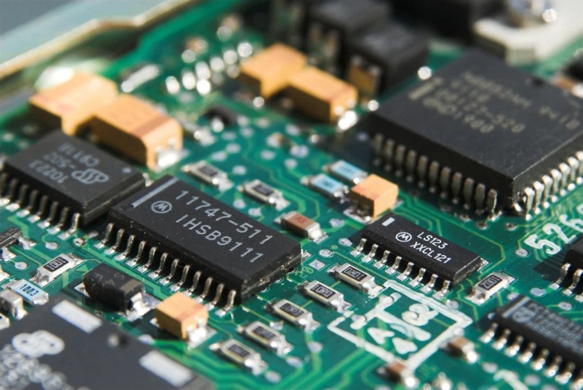
SMD Components
Surface Mount Device (SMD) technology encompasses a wide range of components that are designed to be mounted directly on the surface of a Printed Circuit Board (PCB). These components come in various forms, each serving a specific function in electronic circuits. Let’s explore some of the most commonly used SMD components.
1. Resistors: SMD resistors are small, rectangular-shaped components that provide resistance to the flow of electric current. They are color-coded to indicate their resistance value. SMD resistors come in a variety of sizes and power ratings, making them suitable for a wide range of electronic applications.
2. Capacitors: SMD capacitors store and release electrical energy. They are used to filter out noise, stabilize voltage levels, and store electric charge. SMD capacitors are available in different types, such as ceramic, tantalum, and electrolytic, each with its own set of characteristics and applications.
3. Transistors: SMD transistors are semiconductor devices that amplify or switch electronic signals and power. They come in various types, including bipolar junction transistors (BJTs) and field-effect transistors (FETs), and are widely used in amplifiers, oscillators, voltage regulators, and other electronic circuits.
4. Integrated Circuits (ICs): SMD ICs are complex electronic circuits that integrate multiple functions into a single chip. They range from simple logic gates to highly sophisticated microcontrollers and processors. SMD ICs play a crucial role in modern electronics, serving as the “brain” of various devices.
5. Diodes: SMD diodes are semiconductor devices that allow current to flow in only one direction. They are used for rectification, signal modulation, and voltage regulation. SMD diodes come in different types, such as Schottky diodes, Zener diodes, and light-emitting diodes (LEDs), each with its own specific applications.
6. Inductors: SMD inductors, also known as coils or chokes, store energy in a magnetic field. They are used in various applications, including signal filtering, impedance matching, and power supply regulation. SMD inductors come in different sizes and inductance values to meet the specific requirements of different circuits.
7. Connectors: SMD connectors provide a means to connect various components or modules to the PCB. They allow for easy replacement or removal of components and ensure secure electrical connections. SMD connectors come in different types, including board-to-board connectors, wire-to-board connectors, and flex-to-board connectors.
These are just a few examples of the numerous SMD components available in the electronics industry. Each component plays a vital role in the functionality of electronic devices, and the combined use of these components allows for the creation of innovative and compact electronic products.
Types of SMD Packages
Surface Mount Device (SMD) components come in various package types, each designed to accommodate specific component sizes, shapes, and functionalities. These packages play a crucial role in the assembly and mounting of SMD components onto a Printed Circuit Board (PCB). Let’s explore some of the most commonly used types of SMD packages.
1. Chip Scale Package (CSP): CSP is a highly miniaturized SMD package that offers a high component density. The components in CSP packages are typically mounted directly onto the PCB surface without any additional encapsulation. CSP packages are ideal for applications where space is limited, such as mobile devices, wearable technology, and IoT devices.
2. Quad Flat Package (QFP): QFP is a widely used SMD package characterized by its flat body and leads protruding from all four sides. QFP packages come in a range of sizes, with a higher number of pins available in larger packages. QFP packages are commonly used in applications requiring high pin count, such as microcontrollers, processors, and memory modules.
3. Small Outline Package (SOP): SOP is a compact SMD package with straight leads that extend from the body on two sides. SOP packages are often used in applications where space is limited, such as laptops, televisions, and automotive electronics. They are available in various sizes, including SOP-8, SOP-16, and SOP-28.
4. Ball Grid Array (BGA): BGA is a package type that features an array of solder balls on the bottom of the component. The solder balls create a connection between the package and the PCB. BGA packages offer excellent thermal and electrical performance and are commonly used in high-performance applications, such as graphics processors, networking equipment, and high-density memory modules.
5. Dual In-line Package (DIP): DIP is a through-hole package that was widely used before the rise of SMD technology. However, SMD versions of DIP packages are available, featuring leads that are bent to lie flat against the component body. DIP packages are still used in certain applications that require easy replacement and repair, such as industrial control systems and some consumer electronics.
6. Thin Small Outline Package (TSOP): TSOP is a low-profile SMD package that features a thin body and leads on two sides. TSOP packages are commonly used for memory chips, such as flash memory and RAM modules. They offer significant space savings compared to other packages and provide reliable performance in memory-intensive applications.
7. Plastic-Leaded Chip Carrier (PLCC): PLCC is a square-shaped SMD package with leads arranged on all four sides. PLCC packages are commonly used for integrated circuits and memory chips that require a high number of pins. They offer improved heat dissipation and mechanical stability, making them suitable for demanding applications that require reliable performance.
These are just a few examples of the many SMD package types available today. The choice of the package depends on factors such as component size, pin count, thermal requirements, and the specific application. By utilizing the appropriate package, electronic manufacturers can ensure optimal performance, compact design, and efficient production processes.
SMD Manufacturing Process
The manufacturing process for Surface Mount Device (SMD) components involves several steps that ensure the proper assembly and mounting of these components onto a Printed Circuit Board (PCB). Let’s delve into the key stages of the SMD manufacturing process.
1. PCB Design: The process begins with the design of the PCB, which includes determining the placement and layout of the SMD components. Design software is used to create the PCB layout, including the placement of pads and traces for component connections.
2. Solder Paste Application: Solder paste, a mixture of flux and tiny solder particles, is applied to the designated pads on the PCB. This is typically done through a stencil that allows the accurate deposition of solder paste onto the PCB surface.
3. Component Placement: Once the solder paste is applied, automated pick-and-place machines are used to precisely position the SMD components onto the designated pads. These machines utilize vacuum nozzles to pick up the components and place them onto the correct locations on the PCB, according to the PCB design file.
4. Reflow Soldering: After component placement, the PCB with the SMD components is passed through a reflow oven. The reflow oven subject the PCB to carefully controlled heating, melting the solder paste and forming strong solder joints between the components and the PCB pads. This process typically involves several temperature zones to ensure proper solder melting and reflow.
5. Inspection and Quality Control: Once the soldering process is complete, the PCB undergoes thorough inspection to ensure proper component alignment, solder joint quality, and any potential manufacturing defects. Automated optical inspection (AOI) or X-ray machines are commonly used to detect any discrepancies or defects that may affect the functionality or reliability of the assembled PCB.
6. Cleaning and Testing: After inspection, the PCB may undergo a cleaning process to remove any flux residues or contaminants that may have been left behind during soldering. This ensures a clean and reliable PCB assembly. Following cleaning, functional and electrical testing is conducted to ensure the proper functioning and performance of the assembled SMD components.
7. Post-Assembly Processes: Depending on the specific requirements of the product, additional processes such as conformal coating, encapsulation, or secondary reflow may be performed to protect the PCB and the SMD components from environmental factors or to provide additional functionalities.
The SMD manufacturing process is a highly automated and efficient method that allows for the mass production of electronic devices with smaller form factors and higher component densities. Through precise component placement, controlled soldering, and thorough quality control, manufacturers can produce reliable and high-quality PCB assemblies that meet the demands of various industries.
Soldering SMD Components
Soldering Surface Mount Device (SMD) components onto a Printed Circuit Board (PCB) requires a specialized technique to establish reliable electrical connections. SMD soldering involves the precise placement of components and the application of heat to melt solder and create strong solder joints. Let’s delve into the key steps involved in soldering SMD components.
1. Preparation: Before soldering, it is crucial to prepare both the PCB and the SMD components. The PCB should have the solder pads clean and free from oxidation or contaminants. The SMD components should be handled with proper precautions to prevent damage, such as electrostatic discharge (ESD). An appropriate soldering workstation with the necessary tools, including a soldering iron or a hot air rework station, should be set up.
2. Flux Application: Flux is applied to the solder pads or the component leads to remove oxidation and promote good solder wetting. Flux helps to prevent the formation of solder bridges and ensures proper solder flow during the soldering process. Flux can be applied manually or may already be present in the solder paste used for SMD soldering.
3. Component Placement: SMD components are placed onto the prepared PCB according to the component’s specific orientation and location as specified in the PCB design. Automated pick-and-place machines or manual tweezers are commonly used to place the components accurately onto the solder pads.
4. Soldering Techniques: There are two primary techniques for soldering SMD components: reflow soldering and soldering with a soldering iron. Reflow soldering involves placing the PCB with the components onto a conveyor belt that carries it through a reflow oven. The oven heats the PCB to melt the solder and establish the solder joints. Soldering with a soldering iron involves applying heat directly to the solder pads or the component leads using a specialized soldering iron tip. With proper technique and control, the solder is melted, forming strong solder joints between the components and the PCB.
5. Inspection: After soldering, the PCB should be inspected to ensure well-formed solder joints and the absence of solder bridges or other defects. Automated optical inspection (AOI) or visual inspection under magnification can be used to verify the quality of solder joints. Any necessary touch-up or rework can be performed at this stage to correct any soldering defects and ensure the integrity of the solder connections.
6. Cleaning: If necessary, the soldered PCB may undergo a cleaning process to remove flux residues or contaminants that remain on the surface. Cleaning ensures a clean and reliable PCB assembly. The cleaning technique used should be compatible with the PCB material and the components to avoid damage or corrosion.
Soldering SMD components requires skill, precision, and careful attention to detail. By following proper soldering techniques, manufacturers can create strong and reliable solder joints, resulting in high-quality PCB assemblies. The choice of soldering method, whether reflow soldering or soldering with a soldering iron, depends on factors such as the size of the components, the production volume, and the specific requirements of the electronic device being assembled.
Challenges in Using SMD Components
While Surface Mount Device (SMD) technology offers numerous advantages over traditional through-hole components, it also presents some unique challenges that engineers and manufacturers need to address. Let’s explore some of the common challenges in using SMD components.
1. Size and Handling: The small size of SMD components can make them difficult to handle and place accurately onto the Printed Circuit Board (PCB). The miniature nature of these components requires the use of specialized tools, such as tweezers or vacuum pickup systems, to ensure precise component placement without damaging the components.
2. Heat Management: SMD components are more sensitive to heat than through-hole components due to their compact size and close proximity on the PCB. Heat dissipation becomes critical, and insufficient heat management during soldering can lead to thermal damage or premature component failure. Proper temperature control and adequate cooling measures are essential to mitigate this challenge.
3. Inspection and Rework: SMD components pose challenges in terms of visual inspection, as their size can make it challenging to identify soldering defects or discrepancies. Automated optical inspection (AOI) systems or X-ray machines are often necessary to ensure the quality of solder joints and detect any hidden defects. In the case of rework or repair, the small size and delicate nature of SMD components can complicate the process, requiring skilled technicians and specialized tools.
4. ESD Sensitivity: SMD components are highly susceptible to static electricity. Electrostatic discharge (ESD) can damage or destroy sensitive electronic components, leading to their malfunction or failure. Special precautions, such as utilizing ESD-safe workstations and wearing proper grounding equipment, must be taken to prevent ESD damage during the handling and assembly of SMD components.
5. Component Availability: SMD components are continually evolving, with new technologies and package types emerging regularly. It can sometimes be a challenge to find certain components in the desired package or specifications, particularly for niche or specialized applications. Proper component selection and sourcing are essential to overcome this challenge and ensure the availability of required SMD components.
6. Design Considerations: Designing PCBs for SMD components requires careful consideration of component spacing, trace routing, and signal integrity issues. The compact size and high component density of SMD technology can introduce challenges in PCB layout and routing, and designers need to ensure proper clearance and separation between components to prevent short circuits or signal interference.
Despite these challenges, the benefits of SMD technology far outweigh the difficulties. Addressing these challenges requires expertise, experience, and adherence to best practices in component handling, soldering techniques, inspection, and design considerations. By doing so, engineers and manufacturers can utilize the full potential of SMD components and create reliable and high-performance electronic assemblies.
Common Applications of SMD Technology
The use of Surface Mount Device (SMD) technology has become pervasive in a wide range of industries due to its numerous benefits. Let’s explore some of the common applications where SMD technology is extensively utilized.
1. Consumer Electronics: SMD components are extensively used in consumer electronics, including smartphones, tablets, laptops, televisions, and gaming consoles. The compact size of SMD components allows manufacturers to create sleek and lightweight devices without compromising functionality or performance.
2. Automotive Electronics: SMD technology has revolutionized the automotive industry by enabling the development of advanced electronics systems. SMD components are used in engine control units, infotainment systems, advanced driver-assistance systems (ADAS), and other vehicle systems. Their small size, reliability, and resistance to vibration make them ideal for automotive applications.
3. Communication Systems: SMD components play a vital role in communication systems such as routers, modems, and wireless devices. They are used in high-frequency applications, including RF amplifiers, filters, and antenna modules, ensuring efficient signal transmission and reception.
4. Medical Devices: SMD technology is widely deployed in medical devices, ranging from diagnostics equipment to implantable devices. The compact size of SMD components allows for smaller and more portable medical devices, while their reliability and improved performance ensure accurate and consistent results.
5. Aerospace and Defense: SMD components are crucial in aerospace and defense systems, where compact and lightweight designs are essential. They are used in avionics, guidance systems, radar systems, and satellite electronics. The high-performance and reliability of SMD technology make it well-suited for demanding aerospace and defense applications.
6. Industrial Automation: SMD components are extensively used in industrial automation systems, including programmable logic controllers (PLCs), motor drives, and sensors. Their small size, improved performance, and ability to work in harsh environments contribute to the overall efficiency and reliability of industrial automation systems.
7. Energy Systems: SMD components are integral to energy systems, including renewable energy sources like solar panels and wind turbines. They are utilized in power inverters, battery management systems, and smart grid infrastructure. The higher component density and enhanced thermal characteristics of SMD technology contribute to the overall efficiency and reliability of energy systems.
8. Wearable Technology: SMD components play a crucial role in the development of wearable devices such as fitness trackers, smartwatches, and augmented reality glasses. Their small size, low power consumption, and enhanced performance make them ideal for compact and battery-operated wearable technology.
In summary, SMD technology finds application in numerous industries and is instrumental in creating smaller, more efficient, and reliable electronic devices. From consumer electronics to automotive, aerospace, medical, and industrial applications, SMD components have revolutionized the design and functionality of modern electronic systems, meeting the ever-increasing demands of a technologically advanced world.