
Subatomic Scale: Understanding the Nanometer
The nanometer is a fascinating unit of measurement that plays a crucial role in various fields of science and technology. It represents the subatomic scale, where matter and forces interact at the smallest possible level. To truly understand the significance of this tiny unit, we must delve into its definition, historical background, and the applications it holds in nanotechnology.
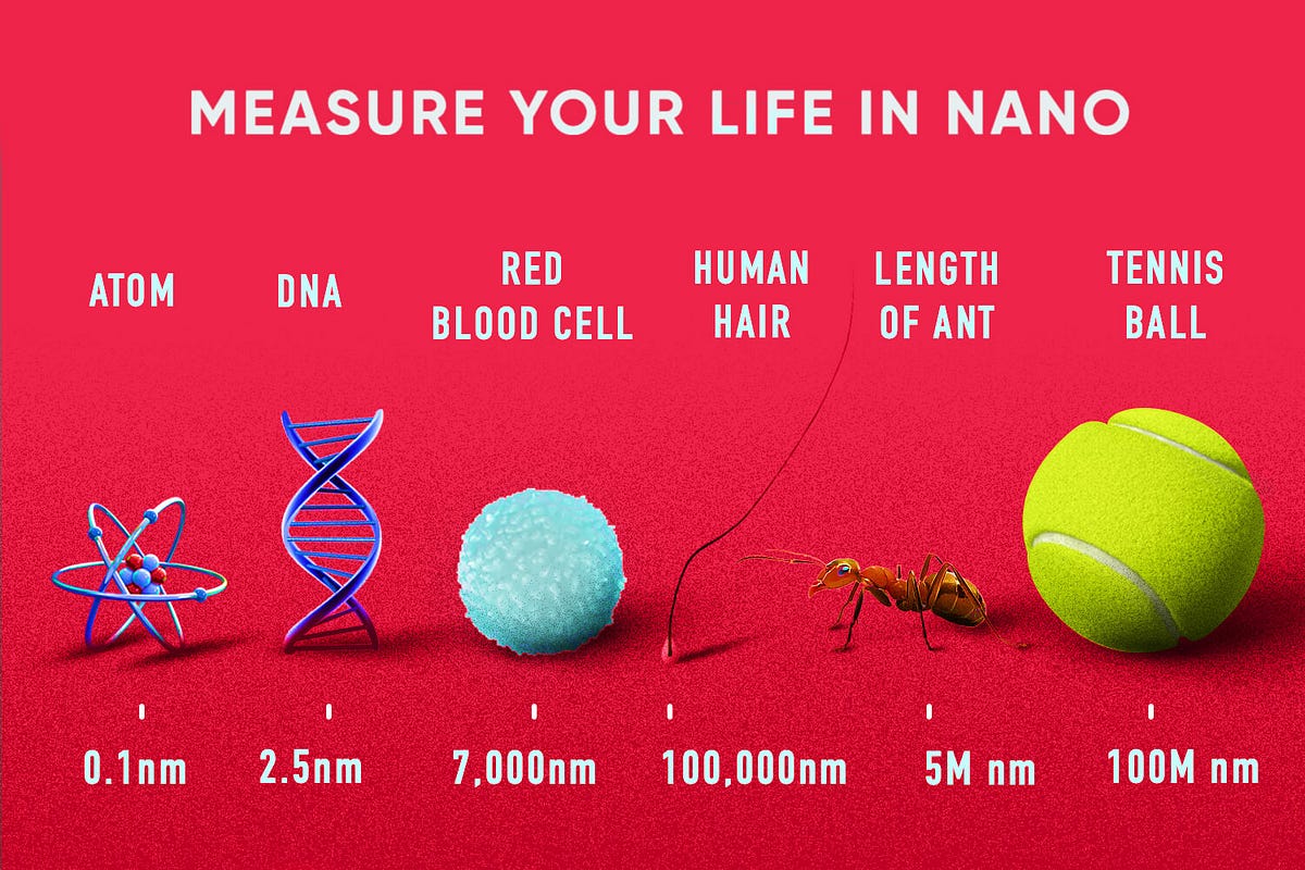
At its core, the nanometer (nm) is equal to one billionth of a meter. To put this into perspective, the average human hair is about 100,000 nanometers wide. It is a remarkably small length scale that often deals with individual atoms, molecules, and the manipulation of their properties.
The concept of the nanometer emerged in the 1960s when scientists realized the need for a unit to describe structures and phenomena on an incredibly small scale. Prior to this, researchers mainly focused on larger units of measurement such as micrometers (one millionth of a meter). With advancements in technology, it became possible to explore and manipulate matter at sizes previously thought to be impossible.
Due to its minuscule size, the nanometer is the perfect scale for various applications in nanotechnology. It is extensively used in the fabrication of nanoscale structures, which can have unique properties and functionalities compared to their larger counterparts. Nanomaterials, such as nanoparticles and nanotubes, exhibit improved electrical, optical, and mechanical properties, making them highly sought after in cutting-edge industries including electronics, medicine, and energy.
Tools that can observe and manipulate nanometers are essential for nanoscale research. Electron microscopes, atomic force microscopes, and scanning tunneling microscopes are some of the remarkable instruments used to explore this minute scale. These tools enable scientists to visualize atomic structures with remarkable precision, aiding in the development of new materials and technologies.
Exploring the nanometer scale also unveils the fascinating world of quantum physics. At such tiny dimensions, quantum effects dominate, and the behavior of particles becomes inherently different from the macroscopic world we are accustomed to. Understanding and harnessing these effects is at the forefront of current scientific research, with potential applications in quantum computing, cryptography, and communication systems.
While the nanometer scale provides us with insights into the building blocks of matter, scientific curiosity continues to push the boundaries further, exploring even smaller units of measurement such as femtometers (one quadrillionth of a meter) and picometers (one trillionth of a meter). The study of these scales unlocks new possibilities in understanding the fundamental laws of nature and developing technologies that were once considered unimaginable.
As we journey into the future, the nanometer will remain a key player in scientific and technological innovations. Its applications and implications extend across various disciplines, shaping the way we perceive and manipulate the world at its most fundamental level. With each new discovery and breakthrough, our understanding of the nanometer expands, opening up endless possibilities for advancements in science, medicine, and technology.
Defining the Nanometer
The nanometer, abbreviated as nm, is a unit of length that represents one billionth of a meter. This tiny scale is the realm of the subatomic, where atoms and molecules interact and the fundamental building blocks of matter are explored. Understanding the definition and significance of the nanometer is key to comprehending the advancements in nanotechnology and the impact it has on various fields of study.
An easy way to visualize the nanometer is by comparing it to the width of a human hair. On average, a human hair is approximately 100,000 nanometers wide. This gives us an idea of just how incredibly small the nanometer is, and the level of precision and technological advancements required to work at this scale.
The nanometer is commonly used in nanotechnology, a field that focuses on manipulating and controlling matter at the nanoscale. At this level, the properties of materials can significantly differ from their bulk counterparts. Nanomaterials exhibit unique characteristics such as enhanced electrical conductivity, enhanced mechanical strength, and increased reactivity, making them ideal for various applications in electronics, medicine, energy, and more.
To put the nanometer in further perspective, let’s consider the size of common objects. A grain of salt is approximately 100,000 to 200,000 nanometers in diameter. The diameter of a red blood cell measures around 6,000 to 8,000 nanometers. Even viruses, which are considered ultra-small, range from 20 to 300 nanometers in size. These examples highlight the significance of the nanometer in terms of representing and manipulating objects at incredibly small scales.
The nanometer is not just a unit of measurement; it is a gateway to the quantum world. At the nanoscale, quantum effects become prominent, and the behavior of particles changes dramatically. This opens up new possibilities for exploring and harnessing quantum phenomena, including quantum entanglement, superposition, and quantum tunneling. These phenomena form the basis of quantum computing, quantum cryptography, and quantum communication, paving the way for revolutionary advancements in information processing and secure communication systems.
To explore and understand matter at the nanoscale, highly sophisticated tools are required. Electron microscopes, atomic force microscopes, and scanning tunneling microscopes allow scientists to observe and manipulate objects at the atomic level. These instruments provide detailed insights into the structure and properties of materials, leading to breakthroughs in nanotechnology research and development.
Historical Background: From Micrometers to Nanometers
The journey from micrometers to nanometers began with the realization that there is a need for a smaller unit of measurement to describe structures and phenomena on a submicron scale. Prior to understanding the nanometer, scientists mainly dealt with the micrometer, which is equivalent to one millionth of a meter or one thousand nanometers.
The concept of the nanometer first came to light in the 1960s when technological advancements enabled researchers to explore and manipulate matter at increasingly smaller scales. As scientific understanding grew, it became apparent that a more precise unit was required to describe materials and phenomena on the atomic and molecular level.
The term “nanometer” derives from the Greek word “nanos,” meaning dwarf or very small. Its adoption as a unit of measurement was a significant step towards understanding and categorizing the world at the submicron scale.
Over time, the development of sophisticated tools and techniques revolutionized our ability to study and work with nanoscale materials. This led to a surge of interest in exploring the properties of matter at the atomic and molecular level, and the nanometer became the standard unit of measurement for these investigations.
One of the key milestones in the advancement of nanotechnology was the invention of the scanning tunneling microscope (STM) in 1981 by Gerd Binnig and Heinrich Rohrer. This powerful instrument allowed scientists to visualize individual atoms and manipulate them on the atomic scale. The invention of the STM, for which Binnig and Rohrer were awarded the Nobel Prize in Physics in 1986, opened up new avenues for research in nanoscience and nanotechnology.
As nanotechnology continued to grow, the importance of the nanometer as a unit of measurement became even more evident. The ability to precisely control and manipulate materials at the nanoscale led to the development of novel nanomaterials with extraordinary properties. These materials have found applications in a wide range of industries, including electronics, medicine, energy, and environmental science.
The historical journey from micrometers to nanometers signifies a paradigm shift in our understanding and manipulation of matter. It represents a transition from focusing on macroscopic features to embracing the intricate world of the submicron scale. This shift has immense implications for the design and development of new technologies that rely on exploiting the unique properties and behaviors of materials at the nanoscale.
As we continue to delve deeper into the nanometer scale, scientific and technological advancements will push the boundaries of what is possible. It is an ongoing journey of discovery that will shape the future of numerous fields, impacting everything from medicine and electronics to energy production and environmental sustainability.
Size Comparison: A Nanometer in Perspective
Understanding the size of a nanometer can be challenging, given its minuscule nature. To put it into perspective, let’s explore some size comparisons that highlight the scale of a nanometer relative to everyday objects and other microscopic entities.
Firstly, consider the width of a human hair, which is typically around 100,000 nanometers. This means that a single strand of hair is about one hundred thousand times thicker than a nanometer. This comparison illustrates the incredible precision needed to work at such a small scale.
Another notable size comparison is the diameter of a red blood cell, which measures around 6,000 to 8,000 nanometers. In other words, hundreds of red blood cells can fit side by side within the span of a single human hair. This demonstrates just how intricately small objects and structures are when measured in nanometers.
Exploring the world of nanoscale, we encounter viruses, which range in size from 20 to 300 nanometers. These tiny infectious particles can only be seen under powerful microscopes, but they play a significant role in diseases and the immune response of organisms. Observing viruses at the nanometer scale allows researchers to comprehend their structure and characteristics, aiding in the development of treatments and vaccines.
Zooming out further, we can compare the nanometer to other units of measurement. One micrometer, equivalent to one millionth of a meter, is roughly 1,000 nanometers. And one millimeter, a commonly used unit, is one million nanometers. This scale comparison shows that a single millimeter encompasses an extraordinary number of nanometers, emphasizing the truly microscopic nature of the nanometer scale.
Considering the progress in technology, it is fascinating to observe how scientists have been able to manipulate individual atoms and molecules at the nanometer scale. The precision and control required to work with such small entities is mind-boggling. Researchers are now able to engineer materials on the atomic scale, creating innovative nanomaterials with exceptional properties and functionalities.
The size comparison of a nanometer with everyday objects and other microscopic entities highlights the immense challenges and opportunities that arise when working at this scale. It emphasizes the importance of advanced tools and techniques, such as electron microscopes and atomic force microscopes, which enable scientists to observe and manipulate objects at the nanometer level.
As we continue to unlock the potential of the nanometer scale, it is essential to appreciate the magnitude of the challenges and achievements that come with working at such a minute level. Exploring and understanding the world of nanometers opens up exciting possibilities for innovation and advancement in various fields, showing that even the tiniest measurements can have a tremendous impact on science, technology, and our daily lives.
Applications in Nanotechnology
Nanotechnology, the manipulation and control of matter at the nanoscale, has revolutionized various fields of study and industry, leading to remarkable advancements and applications. The unique properties and behaviors exhibited by materials at the nanometer scale have resulted in the development of nanomaterials, which are being utilized in a wide range of applications across disciplines.
One of the most promising areas in nanotechnology is electronics. Nanoscale materials, such as nanowires and nanotubes, have exceptional electrical conductivity and mechanical strength. These properties make them ideal for use in miniature electronic devices, such as transistors, sensors, and memory storage. The advancement of nanoelectronics has led to the production of faster and smaller electronic components, revolutionizing the field of computing and communication technology.
In the field of medicine, nanotechnology has opened up new frontiers for drug delivery systems and medical imaging. Nanoparticles, with their large surface area to volume ratio and ability to penetrate cellular barriers, can carry drugs directly to target sites within the body, increasing the efficiency and efficacy of treatments. Additionally, nanoscale imaging agents allow for more precise and detailed imaging of cells and tissues, aiding in early disease diagnosis and monitoring treatment outcomes.
Energy is another area benefiting from nanotechnology. Nanomaterials, such as quantum dots and nanowires, have shown potential in improving the efficiency of solar cells by enhancing light absorption and charge separation. Similarly, nanomaterials are being extensively researched for energy storage applications, enabling the development of high-performance batteries and fuel cells with improved capacity and power output.
The field of materials science is greatly influenced by nanotechnology. Nanocomposites, which are materials composed of a matrix incorporating nanoscale particles, possess enhanced mechanical, thermal, and electrical properties. These materials are used in aerospace applications, construction materials, and even sports equipment. The incorporation of nanoparticles can improve the strength, durability, and stability of materials, leading to improvements and advancements in various industries.
Environmental science has also benefited from nanotechnology. Nanomaterials are being explored for applications in water and air purification systems. The high surface area of nanoparticles allows for efficient removal of pollutants and contaminants from water sources and air, enabling better purification processes. Nanoparticles are also used in environmental sensing and monitoring, aiding in the detection and analysis of pollutants and toxins.
These examples merely scratch the surface of the vast array of applications that nanotechnology offers. From electronics and medicine to energy, materials science, and environmental science, the unique properties of nanoscale materials are revolutionizing industries and opening up unprecedented possibilities. As researchers and scientists continue to explore and understand the intricacies of nanotechnology, its potential for even more remarkable applications is limitless.
Seeing the Unseen: Tools for Observing Nanometers
Observing and understanding objects at the nanometer scale requires advanced tools and techniques that can visualize and manipulate matter on such a minuscule level. Over the years, scientists and researchers have developed remarkable instruments and methods that allow us to explore the nanometer world with unprecedented detail and precision.
One of the essential tools in nanoscale research is the electron microscope. Unlike optical microscopes, which use visible light, electron microscopes utilize a beam of electrons to image samples. The high-energy electron beam allows for greater resolution, enabling scientists to see structures at the atomic scale. Transmission electron microscopes (TEM) and scanning electron microscopes (SEM) are two widely used types of electron microscopes that provide detailed images of materials and allow for the examination of their properties.
Atomic force microscopy (AFM) is another powerful tool used in nanoscale research. It works by scanning a tiny probe over the surface of a sample, detecting the forces between the probe and the surface. This technique can produce three-dimensional images with nanometer resolution, allowing researchers to study surface topography, measure mechanical properties, and manipulate individual atoms or molecules.
Scanning tunneling microscopy (STM) is a fascinating technique that enables the visualization of individual atoms on conductive surfaces. It relies on the quantum tunneling effect, where a sharp tip hovers just above the surface, and a small electric current flows between the tip and the surface. By maintaining a constant current, the tip can follow the contour of the surface, resulting in atomic-level resolution imaging.
Fluorescence microscopy, a widely-used technique in biology and medicine, has also been adapted for nanoscale research. Super-resolution microscopy techniques, such as stimulated emission depletion (STED) microscopy and stochastic optical reconstruction microscopy (STORM), can overcome the diffraction limit of traditional microscopy and achieve resolutions of a few nanometers. This allows for the visualization of cellular structures and processes at an unprecedented level of detail.
The development of these advanced tools has significantly contributed to our understanding of the nanometer scale. They have allowed scientists to observe and manipulate matter with incredible precision, leading to breakthroughs in various fields, including materials science, biology, medicine, and electronics.
As technology continues to advance, new tools and techniques for observing and manipulating nanometers are continuously being developed. The combination of imaging techniques with spectroscopic methods has led to multimodal imaging, where multiple properties and behaviors of materials can be simultaneously visualized and analyzed. These advancements not only provide a more comprehensive understanding of the nanometer world but also open up new avenues for innovation and discovery.
The tools used to observe and manipulate nanometers are the gateway to unlocking the secrets of the nanoscale. With each new advancement, our ability to explore and harness the unique properties of materials at the nanometer level improves, paving the way for groundbreaking discoveries and technological advancements.
The Fabrication of Nanoscale Structures
The creation of nanoscale structures involves a range of sophisticated techniques and processes designed to manipulate matter at the atomic and molecular level. Fabricating structures at such small scales requires precision, control, and the ability to work with extremely delicate materials. The advancements in nanoscale fabrication techniques have fueled the growth of nanotechnology and enabled the development of innovative nanomaterials with unique properties and functionalities.
One of the commonly used techniques for fabricating nanoscale structures is top-down lithography. In this method, a larger material is gradually reduced in size through a series of intricate processes. Photolithography, one of the key techniques, involves projecting light onto a photosensitive material called a photoresist. Through a combination of light exposure, developing, and etching, patterns are formed on the surface, allowing for precise manipulation of structures at the nanometer scale.
Another technique that is widely employed is bottom-up fabrication, where materials are built atom-by-atom or molecule-by-molecule to create nanoscale structures. Self-assembly is a fundamental principle in this approach, where materials have the innate ability to organize themselves into specific patterns or structures. For example, nanocrystals can self-assemble to form ordered arrays, while molecules can be arranged into precise patterns with the aid of templates or chemical interactions.
In addition to top-down and bottom-up approaches, nanoscale fabrication often involves the use of specialized tools and equipment. For instance, focused ion beams (FIB) have revolutionized the field by allowing precise milling, cutting, and deposition of materials at the nanoscale. FIB systems combine high-energy ions with fine-beam control, enabling precise manipulation with sub-nanometer resolution.
Nanopatterning techniques, such as nanolithography and nanoimprint lithography, are employed to create intricate patterns and structures on surfaces. These techniques involve the transfer of patterns from a template onto a substrate, resulting in high-resolution patterns at the nanoscale.
The advancement of nanoscale fabrication techniques has also facilitated the development of 3D nanofabrication methods. Using techniques such as two-photon lithography or electron beam lithography, researchers can create complex three-dimensional structures with unprecedented detail and precision.
Nanoscale fabrication techniques are not limited to traditional solid-state materials. Biological molecules, such as DNA and proteins, can be manipulated and engineered to create nanoscale structures with specific functions. This approach, known as DNA origami, uses the self-assembly properties of DNA to fold it into precise shapes and arrangements, allowing for the creation of custom-designed nanoscale structures.
The fabrication of nanoscale structures is a multidisciplinary field that brings together knowledge and expertise from various disciplines, including physics, chemistry, materials science, and engineering. It is a crucial aspect of nanotechnology, enabling the development of novel materials and devices with enhanced properties and functionalities.
As nanoscale fabrication techniques continue to evolve, the ability to create even smaller and more complex structures becomes a reality. This opens up new possibilities for applications in fields such as electronics, medicine, energy, and environmental science, pushing the boundaries of what is achievable at the nanometer scale.
The Quantum World: Nanometers and Particle Physics
Exploring the nanometer scale delves into the fascinating realm of quantum physics, where the behavior of particles and the fundamental laws of nature take center stage. At the nanometer scale, quantum effects dominate, challenging our understanding of the world and revolutionizing fields such as particle physics and quantum computing.
The study of particles at the nanometer scale provides valuable insights into the building blocks of matter. Many fundamental particles, such as electrons and quarks, have sizes on the order of nanometers. Understanding their properties and interactions is crucial for unraveling the mysteries of the universe.
One of the key concepts in particle physics is wave-particle duality. At the nanometer scale, particles exhibit both particle-like and wave-like characteristics. This means that particles can exist in multiple states simultaneously, a phenomenon known as superposition. The ability to manipulate and exploit this quantum behavior is a cornerstone of emerging technologies like quantum computing. By leveraging superposition and the principles of quantum mechanics, quantum computers have the potential to perform complex calculations exponentially faster than traditional computers.
Quantum entanglement is another fundamental aspect of the nanometer scale. Entanglement occurs when two or more particles become linked in such a way that the state of one particle is intrinsically interconnected with the state of another, even if they are physically separated. This nonlocal connection allows for the possibility of secure communication systems and has profound implications for quantum cryptography.
Nanometer-scale devices and structures are essential for investigating and manipulating quantum phenomena. For instance, quantum dots, nanoscale semiconductors, are used to confine and control the behavior of individual electrons, enabling the creation of qubits – the basic building blocks of quantum computers. Additionally, nanomechanical systems, such as nanowires and nanoresonators, provide a platform for studying quantum effects in macroscopic objects and exploring their potential applications.
Furthermore, the exploration and manipulation of matter at the nanometer scale have played a significant role in particle physics experiments. Particle accelerators and colliders, such as CERN’s Large Hadron Collider, accelerate particles to nearly the speed of light and allow collisions to occur on the nanometer scale. These experiments provide insights into the fundamental forces and particles that make up our universe, helping scientists unravel the mysteries of particle physics and explore new frontiers of knowledge.
As researchers continue to probe the quantum world at the nanometer scale, new discoveries await. The ability to manipulate and control particles and their quantum properties has the potential to revolutionize computing, communication, and our understanding of the universe. Nanometers are the stepping stones to the quantum world, offering a window into the astonishing and mind-bending laws that govern the smallest particles, opening up a universe of possibilities for scientific exploration and technological advancement.
Beyond Nanometers: Exploring Femtometers and Picometers
While the nanometer scale provides valuable insights into the world of atoms and molecules, the exploration of even smaller units of measurement is crucial for pushing the boundaries of our understanding of the universe. Femtometers and picometers, which are smaller than nanometers by orders of magnitude, allow scientists to delve into the intricate and mysterious realm of particle physics and explore the fundamental building blocks of matter.
The femtometer, abbreviated as fm, represents one quadrillionth of a meter, or 10^-15 meters. At this extremely small scale, particle physicists study the behavior and interactions of subatomic particles, including protons, neutrons, and quarks. Understanding these particles is essential for comprehending the fundamental forces that shape our universe.
Particle accelerators, such as the Large Hadron Collider at CERN, play a crucial role in these investigations. These colossal machines accelerate particles to near-light speeds and create collisions at the femtometer scale. By analyzing the results of these collisions, scientists gain insights into the structure of matter and the forces that govern it, providing a deeper understanding of the universe at its most fundamental level.
The picometer, abbreviated as pm, takes the scale even further, representing one trillionth of a meter, or 10^-12 meters. At this scale, scientists examine the intricacies of atomic and molecular interactions. It allows for detailed investigations into bond lengths, atomic radii, and the arrangement of atoms within a molecule.
Advanced spectroscopic techniques, such as X-ray crystallography and nuclear magnetic resonance (NMR) spectroscopy, rely on the picometer scale to determine the precise positions of atoms within a crystal or molecule. These techniques enable scientists to unravel the three-dimensional structures of complex molecules, including proteins and DNA, providing insights into their functions and interactions.
Additionally, picometer-scale measurements are vital for examining the properties of crystals and materials. Characterizing bond lengths and studying the arrangement of atoms within a crystal lattice allows scientists to understand the physical and chemical properties of materials, helping to develop new materials with tailored functionalities.
Exploring the femtometer and picometer scales is essential for deepening our understanding of matter and the universe. It allows us to unravel the intricacies of particles and their interactions and provides insights into the structure and functions of molecules and materials. The exploration of these scales not only expands our knowledge but also opens up possibilities for technological advancements in fields such as medicine, materials science, and quantum technologies.
While the nanometer scale has provided a wealth of knowledge and technological advancements, the pursuit of understanding the universe demands that we go beyond it, venturing into the femtometer and picometer scales. These scales offer a glimpse into the incredible complexity and order that lie hidden within the realm of the infinitesimally small, promising a wealth of discoveries and insights that will continue to shape our understanding of the universe and drive innovation in science and technology.
The Future of Nanometer Research
The field of nanometer research is continually evolving, driven by advancements in technology and our ever-growing understanding of the intricacies of matter at the atomic and molecular scale. As we look to the future, several key areas of focus and potential advancements emerge, shaping the future of nanometer research and its impact on various scientific disciplines.
One of the primary areas of interest is the continued development and exploration of nanomaterials. Researchers are working to discover and engineer new materials with enhanced properties and functionalities that can transform industries such as electronics, medicine, energy, and environmental science. By understanding and controlling the arrangement of atoms and molecules at the nanoscale, scientists can tailor the properties of materials to meet specific needs, leading to leaps in performance, efficiency, and sustainability.
At the intersection of nanotechnology and biology, nanomedicine holds significant promise for the future. Nanoscale drug delivery systems could revolutionize the treatment of diseases by enabling targeted delivery of drugs to specific cells or tissues, reducing side effects and improving therapeutic outcomes. Furthermore, nanosensors and nanoscale diagnostic tools could offer rapid and precise detection of diseases, leading to early intervention and personalized medicine.
Quantum technologies are another area where nanometer research is expected to have profound implications. Quantum computing, in particular, holds the potential to revolutionize data processing, enabling complex calculations and simulations that are currently beyond the reach of traditional computers. Manipulating and controlling qubits, the basic units of quantum information, at the nanoscale is critical for the development of practical quantum computers.
As nanometer research progresses, there is an increasing focus on sustainability and environmental impact. Researchers are exploring the development of eco-friendly nanomaterials and manufacturing processes to ensure that nanotechnology contributes to a greener and more sustainable future. From energy-efficient devices and renewable energy technologies to environmentally friendly water purification systems, nanometer research has the potential to address global challenges and create a more sustainable world.
As technology continues to advance, we can also expect new tools and techniques for nanometer research. Microscopes with even higher resolutions, capable of visualizing individual atoms and molecules, will enable deeper insights into the behavior of matter at the nanoscale. Additionally, advancements in nanofabrication techniques will allow for the creation of even smaller and more complex structures, paving the way for new discoveries and applications.
Collaboration and interdisciplinary research will play a vital role in the future of nanometer research. Bringing together scientists from various fields, including physics, chemistry, materials science, biology, and engineering, will foster innovation and facilitate the development of integrated nanosystems with multi-functional capabilities.