
What Is a Gerber File?
A Gerber file is a type of electronic design data file used in the manufacturing of printed circuit boards (PCBs). It contains a set of instructions that guide the PCB production process, specifying the exact dimensions, placement, and routing of components on the board. Gerber files serve as a universal format that allows PCB manufacturers to accurately reproduce the design created by the PCB designer.
Essentially, a Gerber file acts as a blueprint for the production of a PCB. It provides detailed information about the different layers of the PCB, including the signal traces, copper polygons, solder masks, and silkscreens. By following the instructions in the Gerber file, manufacturers can fabricate the PCB to precise specifications, ensuring that it functions correctly within the intended electronic device.
The Gerber file format is widely recognized and supported by most PCB fabrication facilities across the globe. It has become the industry standard for transferring PCB design data between different software tools and manufacturing processes. This universality makes Gerber files crucial in the efficient and accurate production of PCBs.
In the next section, we’ll explore the purpose of Gerber files in more detail, helping you understand why they play a critical role in PCB manufacturing.
The Purpose of Gerber Files in PCB Manufacturing
Gerber files are essential in the PCB manufacturing process as they serve multiple purposes that ensure the accurate and efficient production of printed circuit boards. Understanding these purposes can provide valuable insights into the significance of Gerber files in the industry.
First and foremost, Gerber files act as a communication tool between PCB designers and manufacturers. They encapsulate the intricate details of the PCB design, such as component placement, trace routing, and layer stack-up. By providing manufacturers with these files, designers can effectively convey their precise design intent, ensuring that the manufactured PCB matches the original design.
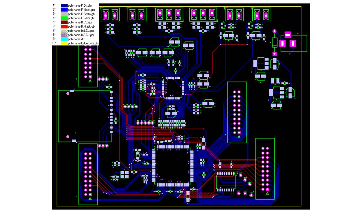
Another purpose of Gerber files is to facilitate the fabrication of different layers of the PCB. Each layer of a PCB, including the copper layers, solder mask, and silkscreen, is represented in a separate Gerber file. These files contain the necessary information for manufacturers to create the physical layers of the PCB accurately. The layer-specific data in Gerber files aids in the proper alignment and registration of different layers during the manufacturing process.
Furthermore, Gerber files play a crucial role in quality control and validation during PCB production. Manufacturers can use Gerber files to conduct Design for Manufacturability (DFM) checks, ensuring that the design follows the manufacturing guidelines and can be produced without errors or difficulties. By verifying the design with Gerber files, potential issues like trace clearance violations or incompatible component footprints can be identified and resolved early in the production process, saving time and reducing costly mistakes.
Additionally, Gerber files enable manufacturers to generate accurate solder masks and silkscreen overlays. The solder mask Gerber file defines the areas of the PCB where solder should not be applied, protecting the underlying copper traces and preventing short circuits. The silkscreen Gerber file, on the other hand, contains information about component designators, part names, and other important markings that aid in board assembly and servicing.
Understanding the Gerber File Format
The Gerber file format is a standardized format used for representing PCB design data. It consists of ASCII text files that contain a series of commands and coordinates that describe the graphical elements and attributes of the PCB design. Understanding how Gerber files are structured and the information they contain is essential for effectively working with them in PCB manufacturing.
A Gerber file is made up of various sections, each serving a specific purpose. These sections include the header section, unit section, aperture definition section, drawing section, and ending section.
The header section provides essential information about the file, such as the file name, creation date, and the unit of measurement used. It also specifies the format version and any additional notes or comments that the designer wishes to include.
The unit section defines the grid or resolution at which the PCB design is represented in the Gerber file. It specifies the measurement unit, such as millimeters or inches, and the precision of coordinates used throughout the file.
The aperture definition section contains a list of predefined apertures or shapes that can be used within the file. Each aperture is defined by its unique identifier, shape, and size. The apertures are used to represent various elements of the PCB design, such as pads, vias, traces, and text.
The drawing section is where the actual graphical elements of the PCB design are defined. It consists of a series of commands and coordinates that specify the placement, size, and attributes of each graphical element. These commands include D-codes that specify the aperture to be used, as well as commands for drawing lines, arcs, circles, polygons, and other shapes.
The ending section marks the end of the Gerber file and may include any final comments or notes from the designer.
Throughout the file, the Gerber format uses a coordinate system based on the chosen unit of measurement. The coordinates specify the X and Y positions of each graphical element, allowing for precise placement on the PCB.
By understanding the structure and content of Gerber files, manufacturers can accurately interpret and translate the design data into physical PCBs. Designers can also ensure that their intentions are accurately represented in the Gerber file, leading to the desired outcome during PCB fabrication.
How to Generate Gerber Files from PCB Design Software
Generating Gerber files from PCB design software is a crucial step in preparing a design for manufacturing. Most PCB design software packages offer built-in functionalities to generate Gerber files. Here’s a step-by-step guide on how to generate Gerber files from popular PCB design software:
- Step 1: Open your PCB design project in the PCB design software of your choice.
- Step 2: Verify that your design is fully complete and error-free. Make sure all the components are placed correctly and all connections are properly routed.
- Step 3: Access the ‘Export’ or ‘Generate’ option in the software. This option is usually found in the ‘File’ or ‘Fabrication Outputs’ menu.
- Step 4: Within the export options, select the Gerber file format as the output file type. Some software may provide options for selecting the specific layers or components to export.
- Step 5: Configure the export settings according to your manufacturing requirements. This may include specifying the units (e.g., millimeters or inches) and the resolution or precision of the Gerber files.
- Step 6: Review the export summary to ensure that all the necessary layers, apertures, and other design elements are included in the Gerber file generation.
- Step 7: Choose the destination folder or location where the Gerber files will be saved.
- Step 8: Initiate the export process and allow the software to generate the Gerber files. This may take a few moments depending on the complexity of the design.
- Step 9: Once the Gerber files are generated, review them to confirm that all the design elements and layers are correctly represented.
- Step 10: As an optional but recommended step, use Gerber file viewer software to open and examine the exported files. This helps ensure that the Gerber files appear as expected and can be properly interpreted by PCB manufacturers.
By following these steps, you can easily generate Gerber files from your PCB design software, providing manufacturers with the necessary data to produce your PCB accurately and efficiently.
The Components of a Gerber File
A Gerber file consists of several components, each of which provides specific information about the design of a printed circuit board (PCB). Understanding the different components of a Gerber file is essential for accurately interpreting and manufacturing the PCB. Let’s explore the key components of a Gerber file:
- Header: The header section of a Gerber file contains general information about the file, such as the file format version, creation date, and additional notes or comments from the designer.
- Unit Definition: The unit section specifies the measurement unit used in the Gerber file, such as millimeters or inches. It also defines the resolution or precision of the coordinates used throughout the file.
- Aperture Definitions: Aperture definitions define the shapes and sizes of different elements in the PCB design. Each aperture is assigned a unique identifier and includes attributes such as shape, size, and rotation angle.
- Drawing Commands: The drawing section contains a series of commands that represent the graphical elements of the PCB design. These commands include D-codes, which specify the aperture to be used, and X-Y coordinates that define the position of the elements.
- Ending: The ending section marks the end of the Gerber file and may include additional comments or notes.
Within the drawing commands, there are different types of elements that make up the PCB design:
- Lines: Lines are commonly used to represent conductive traces on the PCB. They are defined by their start and end coordinates, width, and other attributes.
- Polygons: Polygons are closed shapes with multiple sides, often used to represent copper pour areas or filled regions on the PCB. They are specified by a series of vertices.
- Circles and Arcs: Circles and arcs are utilized to represent components, holes, or rounded traces on the PCB. They are defined by their center coordinates, radius, and angles.
- Text: Text elements include designators, part names, symbols, or other labels that provide additional information about the PCB design. They are defined by their position, font style, height, and orientation.
By understanding these components, manufacturers can accurately interpret and translate the Gerber file data into the physical PCB. Designers can also review and validate the Gerber files to ensure that the desired design elements are accurately represented, leading to successful PCB fabrication.
Viewing Gerber Files: A Step-by-Step Guide
Viewing Gerber files is an important step in the PCB manufacturing process. It allows designers and manufacturers to inspect the graphical representation of the PCB design before proceeding with fabrication. To view Gerber files, you can follow this step-by-step guide:
- Step 1: Obtain a Gerber file viewer software. There are various free and commercial options available, such as Gerbv, ViewMate, and GC-Prevue.
- Step 2: Install the Gerber viewer software on your computer.
- Step 3: Open the Gerber viewer software.
- Step 4: Locate the Gerber files you want to view on your computer.
- Step 5: In the Gerber viewer software, navigate to the ‘File’ or ‘Open’ menu option.
- Step 6: Select the Gerber file(s) you wish to view and click ‘Open’.
- Step 7: The Gerber viewer software will display the PCB design in a graphical format. You can zoom in/out and pan to examine different areas of the design.
- Step 8: Use the viewer’s tools and functionalities to inspect various aspects of the design, such as individual layers, trace routing, component placement, and solder mask locations.
- Step 9: Take advantage of measurement tools provided by the Gerber viewer to check dimensions, distances, or clearance between design elements, ensuring they meet your requirements.
- Step 10: If necessary, toggle between different layers, view solder mask and silkscreen overlays, and modify the view settings to suit your needs.
By following these steps, you can effectively view and examine Gerber files, gaining valuable insights into the PCB design and identifying any potential issues or discrepancies before moving forward with PCB manufacturing.
Opening Gerber Files with Gerber Viewers
To open Gerber files, you can use specialized Gerber viewer software. Gerber viewers allow you to visualize and analyze the content of Gerber files, making them essential tools for PCB designers and manufacturers. Here’s a step-by-step guide on how to open Gerber files using Gerber viewers:
- Step 1: Install a Gerber viewer software on your computer. There are several options available, such as Gerbv, ViewMate, GC-Prevue, and more.
- Step 2: Launch the Gerber viewer software after installation.
- Step 3: Locate the Gerber files you want to open on your computer. Ensure that the Gerber files are stored in a location that is accessible by the Gerber viewer software.
- Step 4: In the Gerber viewer software, go to the ‘File’ or ‘Open’ menu option.
- Step 5: Specify the Gerber file(s) you want to open in the file selection dialogue box.
- Step 6: Click ‘Open’ or ‘OK’ to load the Gerber file(s) into the viewer.
- Step 7: The Gerber viewer will display the content of the Gerber file(s) in a graphical format. You can navigate through the layers and zoom in/out to examine specific areas of the design.
- Step 8: Take advantage of the viewer’s features to analyze the design, such as measuring distances between design elements, inspecting trace routing, or verifying component placements.
- Step 9: Use additional functionalities provided by the Gerber viewer to toggle between layers, view solder mask and silkscreen overlays, and customize the viewing settings to your preference.
- Step 10: When you have finished reviewing the Gerber files, you can save any changes or annotations made within the Gerber viewer, if supported by the software.
Opening Gerber files with Gerber viewers allows for detailed examination and analysis of the PCB design, helping designers and manufacturers ensure accuracy and identify any potential issues before moving forward with the manufacturing process.
Gerber File Integrity: Tips for Ensuring Accuracy
Ensuring the integrity of Gerber files is crucial in the PCB manufacturing process. Accuracy and reliability are essential to avoid costly errors during fabrication. Here are some tips to help you maintain the integrity of Gerber files:
- Validate the Design: Before generating Gerber files, thoroughly review and validate your PCB design in the PCB design software itself. Confirm that all components are correctly placed, connections are properly routed, and there are no design rule violations.
- Use Trusted PCB Design Software: Work with reputable and reliable PCB design software that supports the Gerber file format. Ensure that the software is up to date to minimize the risk of bugs or compatibility issues that may affect Gerber file generation.
- Double-Check Export Settings: When exporting Gerber files, carefully review the export settings. Confirm that the correct layers, resolutions, and units are selected. Double-check the parameters to ensure they match your manufacturing requirements.
- Inspect Gerber Files with a Viewer: Before sending Gerber files to the manufacturer, use a Gerber file viewer to inspect the files. Verify that the layers, components, and design elements are accurately represented. Pay attention to details such as trace clearances, pad sizes, and solder mask openings.
- Perform Design Rule Checks (DRC): Use DRC tools in your PCB design software or Gerber viewer to run design rule checks. This helps identify potential issues or violations, such as inadequate clearances, overlapping objects, or incorrect pad sizes.
- Collaborate with the Manufacturer: Communicate with your PCB manufacturer early in the design process. Understand their capabilities and requirements to ensure your Gerber files align with their manufacturing processes. Seek their expertise to validate your design and prevent any production challenges.
- Backup Gerber Files: Always keep backup copies of your Gerber files in a secure location. Accidents or data loss can occur, so having backups will prevent potential disruptions in the manufacturing process.
- Regularly Update and Maintain Design Software: Stay up to date with the latest version of your PCB design software. Updates often include bug fixes, performance improvements, and enhanced Gerber file generation. Regular maintenance ensures accuracy and compatibility with manufacturing requirements.
By following these tips, you can enhance the integrity and accuracy of your Gerber files, minimizing errors, and ensuring a smooth and successful PCB manufacturing process.
Converting Gerber Files to Other Formats
In addition to the Gerber file format, there may be situations where it is necessary to convert Gerber files to other formats. Conversion can be useful for compatibility with different software tools, collaboration with others, or specific manufacturing requirements. Here are some common methods for converting Gerber files to other formats:
- DXF/DWG: DXF (Drawing Exchange Format) or DWG (Drawing) files are commonly used in computer-aided design (CAD) software. To convert Gerber files to DXF or DWG, various conversion utilities or plugins are available. These tools extract the necessary data from the Gerber files and convert them into a compatible format for use in CAD applications.
- ODB++: ODB++ is an alternative format widely adopted in the PCB industry. It provides a comprehensive representation of the PCB design, including all necessary manufacturing data. Some PCB design software includes built-in options to export Gerber files as ODB++, or standalone conversion software can be used to convert Gerber files to ODB++ format.
- IPC-2581: IPC-2581 is an industry standard XML-based format for PCB manufacturing data exchange. It integrates all design and manufacturing-related information into a single file. Conversion tools are available to convert Gerber files to IPC-2581 format, enabling seamless data transfer between different software platforms and manufacturing processes.
- PDF: Portable Document Format (PDF) files offer an easy way to share PCB design information with stakeholders who may not have access to specialized CAD software. To convert Gerber files to PDF, you can use software that allows printing or exporting Gerber files as PDF documents. This conversion preserves the graphical representation of the PCB design and makes it easily viewable and shareable.
- Other PCB Design Software Formats: Depending on your specific requirements, you may need to convert Gerber files to other PCB design software formats such as Altium Designer (.PCBDOC), Eagle (.BRD), or KiCad (.KICAD_PCB). In such cases, file conversion utilities or import/export functions within the respective software tools can enable the conversion process.
It’s important to note that when converting Gerber files to other formats, there may be limitations and considerations to keep in mind. Some data, such as aperture definitions or specific layer information, may not be easily preserved in the conversion process. Therefore, it’s recommended to thoroughly review and validate the converted files to ensure the accuracy and completeness of the converted data.
By utilizing the appropriate conversion methods, you can effectively convert Gerber files to other formats, enhancing compatibility, collaboration, and meeting the specific requirements of your PCB design and manufacturing workflow.
Gerber Files and PCB Manufacturing: Best Practices
When it comes to using Gerber files in PCB manufacturing, following best practices can help ensure a seamless and successful production process. These practices help maintain the accuracy and integrity of the Gerber files, minimize errors, and facilitate efficient communication between designers and manufacturers. Here are some essential best practices to consider:
- Collaborate Early: Engage in open communication with your PCB manufacturer from the early stages of the design process. Discuss design intent, manufacturing capabilities, and any specific requirements that may affect the Gerber file generation.
- Choose the Correct Layers: Ensure that you select the correct layers for your Gerber files. Review and verify that all required layers, including copper, solder mask, silkscreen, and drill data, are included. Missing or incorrect layers can lead to critical errors during production.
- Verify Design Rule Compliance: Run design rule checks (DRCs) on your PCB design software to identify any potential violations. Confirm that the design follows your manufacturer’s specifications regarding trace clearances, pad sizes, minimum hole sizes, and other design rules.
- Review Aperture Definitions: Carefully define apertures for each design element in your Gerber files. Verify the aperture settings and ensure that they accurately represent the specific design requirements, such as pad shapes, hole sizes, or solder mask openings.
- Double-Check File Naming: Use clear and consistent file naming conventions for your Gerber files. Avoid special characters, spaces, or excessively long file names, as they may cause compatibility issues with certain manufacturing software or equipment.
- Provide Clear Documentation: Accompany your Gerber files with clear and detailed documentation. Include important information such as component footprints, layer stack-ups, manufacturing notes, and any specific instructions or special considerations for the PCB assembler.
- Validate Gerber Files: Before sending Gerber files to the manufacturer, validate them using a Gerber viewer. Confirm that the design elements, layers, pad sizes, and overall representation of the PCB match your intentions.
- Backup Gerber Files: Keep backup copies of your Gerber files in a secure location. This ensures that you have a reliable source to revert to if any issues arise during the manufacturing process or in case of accidental file loss.
- Follow Manufacturer Guidelines: Adhere to the fabrication guidelines provided by your manufacturer. Review their specifications for preferred formats, layer order, and any restrictions or requirements specific to their equipment and processes.
- Communicate with the Manufacturer: Maintain open lines of communication with your manufacturer throughout the manufacturing process. Address any questions or concerns promptly to ensure a smooth collaboration, minimize delays, and achieve the desired outcome for your PCB design.
By implementing these best practices, you can optimize the use of Gerber files in PCB manufacturing, promoting accuracy, efficiency, and a successful production process.