
html
What is a Die in Electronics?
A die in electronics refers to the small, rectangular piece of a semiconductor material upon which integrated circuits (ICs) are fabricated. It is the foundation of modern electronic devices and is responsible for the magic that happens inside our smartphones, computers, and other high-tech gadgets. The concept of a die is fundamental to the field of microelectronics and plays a crucial role in the design, manufacturing, and functioning of electronic devices.
The die is essentially a miniaturized version of the finished electronic component, such as a microprocessor or memory chip. It contains all the necessary components, including transistors, resistors, capacitors, and interconnects, that enable the device to perform specific functions. Think of it as the heart and brain of the electronic device, controlling and processing data in a rapid and efficient manner.
One of the key characteristics of a die is its small size. It typically measures a few millimeters on each side, although in some advanced semiconductor technologies, the size can be reduced to a few micrometers or even nanometers. This miniaturization allows for more components to be packed into a smaller space, resulting in faster and more powerful electronic devices.
The construction of a die involves a complex process known as semiconductor fabrication, or simply, chip manufacturing. This process involves depositing and patterning layers of different materials on a silicon wafer to create the desired circuitry. The precision and accuracy required in this process are critical as even the tiniest defect or misalignment can render the die unusable.
Once the die is fabricated, it undergoes extensive testing and quality control measures to ensure that it meets the required specifications. This includes checking for defects, such as open or short circuits, and verifying the functionality of the integrated circuits. Only the dies that pass these tests are further packaged and assembled into complete electronic components.
The die is then housed in a protective package that provides mechanical support and electrical connections to the external world. This packaging process not only protects the delicate die from damage but also allows for easy integration into electronic devices. Different packaging options, such as ceramic packages or plastic encapsulation, are available depending on the specific requirements of the application.
The use of semiconductor dies has revolutionized the field of electronics and has paved the way for countless advancements in technology. From smartphones and computers to automotive systems and medical devices, semiconductor dies are omnipresent in the modern world. Their small size, high performance, and reliability make them an ideal choice for a wide range of applications.
However, it is essential to note that semiconductor dies also have some disadvantages. The fabrication process is highly complex and requires sophisticated equipment and expertise, making it expensive. Additionally, the shrinking size of dies brings new challenges in terms of heat dissipation and power management.
Despite these challenges, the use of semiconductor dies continues to drive innovation in the electronics industry. As technology advances and demands for smaller, faster, and more efficient devices increase, the importance of die design and manufacturing will only grow.
html
History of Semiconductor Dies
The history of semiconductor dies dates back to the mid-20th century when the field of microelectronics was taking its first steps. The development of the first practical semiconductor transistor in the late 1940s paved the way for the miniaturization of electronic components and the birth of the integrated circuit.
In the early days, integrated circuits were fabricated using individual transistors, resistors, and diodes that were wire-bonded onto a ceramic substrate. These components were relatively large and bulky, limiting the complexity and performance of electronic devices. However, advancements in semiconductor manufacturing techniques soon led to the evolution of the die.
In the late 1950s and early 1960s, researchers at companies like Texas Instruments and Fairchild Semiconductor made groundbreaking discoveries that laid the foundation for the modern semiconductor industry. They developed the concept of planar transistor structures and introduced silicon as the primary material for semiconductor fabrication.
By the 1960s, integrated circuits were being fabricated on small slices of silicon known as wafers. These wafers were divided into individual dies, each containing multiple transistors and interconnects. The dies were then wire-bonded to a lead frame and encapsulated in plastic or ceramic packages to create complete electronic components.
Over the years, the size of semiconductor dies has continued to shrink dramatically, thanks to advancements in lithography and etching techniques. This has allowed for the integration of more components and increased functionality in smaller spaces. The introduction of strain engineering, high-k dielectric materials, and FinFET transistors further enhanced the performance and power efficiency of semiconductor dies.
Additionally, the development of 3D packaging technologies, such as stacked dies and system-in-package (SiP), has enabled even more compact and integrated electronic devices. These advances have fueled the growth of the semiconductor industry and have led to the proliferation of smartphones, tablets, wearable devices, and other electronics.
Looking ahead, the future of semiconductor dies is likely to be driven by advancements in nanotechnology and emerging technologies such as quantum computing and flexible electronics. These innovations hold the promise of further miniaturization and increased functionality, opening up a world of possibilities for next-generation electronic devices.
html
Structure of a Semiconductor Die
The structure of a semiconductor die is a marvel of engineering and precision. It is meticulously designed to include all the necessary components and interconnections required for the proper functioning of the integrated circuit.
A typical semiconductor die consists of multiple layers of different materials, each serving a specific purpose. The most common material used is silicon, due to its excellent electrical properties. Other materials, such as metals and insulators, are also utilized to create the desired circuitry.
The most fundamental component of a die is the transistor. Transistors are the building blocks of digital circuits and are responsible for amplifying and switching electrical signals. Depending on the complexity of the design, a single die can contain thousands or even millions of transistors.
In addition to transistors, a die also incorporates other passive components, such as resistors, capacitors, and diodes. These components are used to control and manipulate signals in the circuit, enabling various functions like storing data, filtering signals, and providing power regulation.
The interconnections between these components are crucial for the proper operation of the integrated circuit. These interconnections, known as interconnects or wiring layers, are typically made of metal, such as copper or aluminum. They allow for the transmission of signals and power between different components on the die.
The wiring layers are patterned using advanced lithography techniques, creating intricate pathways that connect the various components together. These pathways are carefully designed to minimize signal interference, crosstalk, and power losses, ensuring optimal performance of the integrated circuit.
Modern semiconductor dies also incorporate specialized structures to enhance performance and reduce power consumption. For example, strained silicon technology introduces controlled mechanical strain to the silicon crystal lattice, improving the mobility of electrons and increasing transistor performance.
The die is further structured with multiple layers of insulating materials to isolate and protect the various components from each other. These insulating layers, typically made of materials like silicon dioxide or silicon nitride, prevent unintended electrical interactions and ensure the reliability and longevity of the integrated circuit.
The overall size and shape of the semiconductor die vary depending on the specific application and design requirements. Miniaturization has been a key trend, with constant efforts to reduce the size of dies to accommodate the demand for smaller and more powerful electronic devices.
In summary, the structure of a semiconductor die is a carefully engineered combination of active and passive components, interconnections, and insulating layers. It is optimized for performance, reliability, and miniaturization, making it a critical element in the world of microelectronics.
html
Materials Used in Semiconductor Dies
Various materials are used in the fabrication of semiconductor dies, each with specific properties that contribute to the performance and functionality of the integrated circuit.
One of the most widely used materials in semiconductor manufacturing is silicon. Silicon is a semiconductor material that possesses excellent electrical properties, such as high carrier mobility and a wide bandgap. It is abundantly available and can be easily processed into wafers, which serve as the starting point for die fabrication.
In addition to silicon, metals are essential for interconnects and contacts in the integrated circuit. Common metals used include copper, aluminum, and gold – each chosen for its conductivity and compatibility with the fabrication process. These metals are patterned and deposited onto the die using techniques like physical vapor deposition (PVD) or chemical vapor deposition (CVD).
Insulating materials are also crucial in die construction, and silicon dioxide (SiO2) is a commonly used insulator due to its excellent electrical insulation properties. In advanced semiconductor technologies, other insulating materials like silicon nitride (Si3N4) and high-k dielectrics, such as hafnium oxide (HfO2) or zirconium oxide (ZrO2), are employed to control leakage current and improve the performance of transistors.
To enhance the performance of transistors, semiconductor manufacturers often introduce dopants into the silicon crystal lattice. These dopants modify the electrical properties of silicon, allowing for the creation of n-type (electron-rich) and p-type (hole-rich) regions, essential for transistor operation.
In recent years, the development of new materials has played a significant role in advancing semiconductor technology. For example, gallium arsenide (GaAs) and indium phosphide (InP) are used in specialized applications where high-frequency operation or high-speed switching is required.
Furthermore, materials like germanium (Ge) and III-V compound semiconductors (e.g., gallium nitride, GaN) are employed in emerging technologies like optoelectronics and power electronics. These materials offer unique properties, such as high electron mobility or excellent light-emitting capabilities, allowing for the development of advanced devices.
The selection of materials for a semiconductor die depends on various factors, including the intended application, performance requirements, and cost considerations. Semiconductor manufacturers constantly strive to identify and utilize materials that offer better performance, lower power consumption, and higher reliability.
As technology continues to advance, researchers are exploring new materials, such as graphene and carbon nanotubes, to overcome the limitations of traditional materials and push the boundaries of semiconductor technology even further.
html
Manufacturing Process of Semiconductor Dies
The manufacturing process of semiconductor dies, also known as chip fabrication or semiconductor fabrication, involves a series of intricate steps that transform a silicon wafer into a functional integrated circuit.
The process begins with the selection of a high-purity silicon wafer. These wafers are typically made from highly crystalline silicon and are meticulously cleaned to remove any contaminants or particles.
Once the wafer is prepared, a series of fabrication steps, often referred to as front-end-of-line (FEOL) processing, are performed to create the basic structure of the integrated circuit. This includes steps such as oxidation, in which a layer of silicon dioxide is grown on the wafer surface, and photolithography, where the desired patterns are formed using a selective masking process.
The next step involves the deposition of various materials onto the wafer to form the different layers and components of the integrated circuit. This can be done through techniques like physical vapor deposition (PVD), chemical vapor deposition (CVD), or atomic layer deposition (ALD), depending on the specific requirements of the design.
After deposition, these layers are patterned using photolithography and etching processes. Photolithography involves exposing the wafer to ultraviolet light through a mask, which defines the desired patterns. The exposed areas are then chemically or plasma-etched to remove or modify the material selectively, creating the desired features on the wafer.
As the fabrication process progresses, additional layers are deposited and patterned to create the transistors, interconnects, and other components of the integrated circuit. This may involve the use of additional masking steps and specialized fabrication techniques like ion implantation or epitaxial growth.
Throughout the fabrication process, each step is carefully monitored and controlled to ensure the accuracy and quality of the integrated circuit. Advanced tools and metrology techniques are employed to measure critical dimensions and characterize the electrical performance of the fabricated components.
Once the fabrication of the dies is complete, they undergo testing and quality control measures to verify their functionality and adherence to the required specifications. Testing techniques, such as wafer probing and electrical testing, are performed to identify any defects or failures before the dies can proceed to the packaging stage.
The packaging of the semiconductor dies is the final step in the manufacturing process. This involves encapsulating the dies in protective packages that provide mechanical support and electrical connections to the external world. Different packaging options, such as ceramic packages or plastic encapsulation, are available depending on the specific requirements of the application.
Overall, the manufacturing process of semiconductor dies requires advanced equipment, techniques, and expertise. It is a highly intricate and precise process that plays a crucial role in the production of modern integrated circuits, enabling the development of powerful and advanced electronic devices.
html
Testing and Quality Control of Semiconductor Dies
Testing and quality control play a vital role in ensuring the reliability and functionality of semiconductor dies. The complex nature of semiconductor fabrication makes it essential to implement rigorous testing procedures throughout the manufacturing process to identify and rectify any potential defects or issues.
The testing process begins after the fabrication of the semiconductor dies is complete. One common testing method is wafer probing, where the electrical characteristics of each die are measured using specialized equipment that makes contact with the specific pads on the wafer. This allows for the identification of any defective dies or circuitry on the wafer.
After wafer probing, the good dies are typically singulated from the wafer by dicing them into individual units. These individual dies then undergo further testing to ensure their functionality and performance before they can be integrated into electronic devices.
Electrical testing is a critical aspect of die testing. Various tests, including functional testing, parametric testing, and performance testing, are conducted to verify that the integrated circuits meet the required specifications. These tests assess the performance of different components on the die, such as transistors, interconnects, and memory cells, and ensure that they operate within specified ranges.
In addition to electrical testing, visual inspection and microscopic examination are also performed to identify any physical defects on the die’s surface or within its circuitry. This includes checking for defects like cracks, broken bonds, or contamination, which can impact the functionality and reliability of the die.
The quality control process extends beyond testing individual dies. Statistical process control (SPC) techniques are employed to monitor and analyze the entire manufacturing process to identify any process variations or deviations that may affect the quality of the dies. This proactive approach allows manufacturers to detect and rectify issues early on, ensuring the production of high-quality dies.
A key aspect of quality control is the use of quality metrics and standards. Quality metrics, such as defect density and yield rate, provide valuable insights into the overall quality of the fabrication process. Compliance with international quality standards, such as the International Organization for Standardization (ISO) standards or the Automotive Electronics Council (AEC) standards, helps ensure that the semiconductor dies meet the required industry guidelines for reliability and performance.
The advent of automated testing equipment (ATE) and sophisticated testing algorithms has significantly improved the efficiency and accuracy of die testing. These advancements enable faster and more comprehensive testing, allowing for higher production yields and reduced costs.
In summary, testing and quality control are essential for guaranteeing the functionality, reliability, and performance of semiconductor dies. Through a combination of electrical testing, visual inspection, statistical analysis, and adherence to international quality standards, manufacturers can ensure that only high-quality dies make their way into the final electronic devices.
html
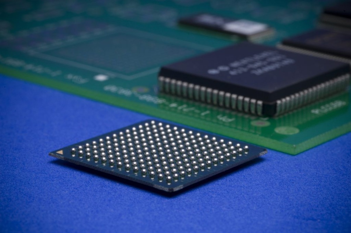
Packaging and Assembly of Semiconductor Dies
The packaging and assembly of semiconductor dies are critical steps in the manufacturing process that ensure the protection, electrical connectivity, and integration of the dies into electronic devices.
Once the semiconductor dies have passed the testing and quality control stage, they are ready to be packaged. Packaging provides mechanical support and protection to the delicate silicon dies, shielding them from environmental factors like moisture, dust, and mechanical stress.
There are various packaging options available, depending on the specific requirements of the application. Ceramic packages, which offer excellent heat dissipation and durability, are often used in high-performance applications such as microprocessors. Plastic encapsulation, on the other hand, provides cost-effective and versatile packaging for a wide range of consumer electronics.
The packaging process involves placing the die onto a lead frame or substrate, which provides electrical connections to the outside world. This is typically done using wire bonding or flip-chip bonding techniques. Wire bonding uses thin gold or aluminum wires to create electrical connections between the bonding pads on the die and the lead frame. Flip-chip bonding, on the other hand, involves directly soldering the die onto the substrate, allowing for higher-density interconnections and improved electrical performance.
After bonding, the die is typically encapsulated in a protective material, such as epoxy or plastic molding compound. This encapsulation not only provides additional protection but also ensures the long-term reliability and durability of the package.
During the packaging process, additional components, such as passive components or surface-mounted devices (SMDs), may be added to the package to enhance functionality or provide additional features. These components are bonded to the die or substrate using techniques like surface mount technology (SMT) or wire bonding, allowing for the integration of multiple functions within a single package.
Once the packaging and assembly process is complete, the packaged semiconductor dies are subjected to further testing to verify their functionality and ensure the integrity of the connections. This includes tests like package electrical testing, reliability testing, and thermal cycling, which assess the performance and reliability of the packaged dies under different operating conditions.
The packaged semiconductor dies are then ready for integration into electronic devices. They can be mounted onto printed circuit boards (PCBs) using techniques like surface mount technology (SMT) or through-hole mounting, depending on the specific requirements of the application.
In summary, the packaging and assembly of semiconductor dies are crucial steps in the overall manufacturing process. They provide protection, electrical connectivity, and integration of the dies into electronic devices. By employing advanced packaging techniques and thorough testing, manufacturers ensure the reliability, functionality, and longevity of the final electronic products.
html
Applications of Semiconductor Dies
Semiconductor dies have revolutionized the field of electronics and have become an integral part of numerous everyday devices and technologies across various industries. The advancements in semiconductor technology have enabled the creation of smaller, faster, and more efficient electronic components, opening up a wide range of exciting applications.
One of the most prominent applications of semiconductor dies is in the field of consumer electronics. From smartphones and tablets to laptops and smartwatches, semiconductor dies form the backbone of these devices, enabling features like high-speed processors, memory storage, and wireless connectivity. The miniaturization of semiconductor dies has made it possible to create compact and powerful devices that have transformed the way we communicate, work, and access information.
Semiconductor dies are also crucial in the automotive industry, advancing the functionality and safety of vehicles. They are used in various applications such as engine control units (ECUs), advanced driver-assistance systems (ADAS), and infotainment systems. These dies provide the computational power and control necessary for features like fuel efficiency optimization, collision avoidance, and in-vehicle entertainment.
In the healthcare sector, semiconductor dies are utilized in medical devices and equipment. They enable advancements in diagnostic imaging, patient monitoring systems, and implantable medical devices. Semiconductor dies with wireless connectivity capabilities are also used in telemedicine applications, allowing for remote monitoring and consultations.
Industrial automation and control systems heavily rely on semiconductor dies for precise control and monitoring. They are used in programmable logic controllers (PLCs), sensors, and actuators, enabling automation and optimization of industrial processes. The high-performance capabilities of semiconductor dies enhance productivity, efficiency, and safety in manufacturing and industrial settings.
The energy sector is another area where semiconductor dies find extensive use. They are vital in renewable energy systems, such as solar cells and wind turbines, where they convert and manage energy efficiently. Semiconductor dies are also used in power electronics applications, including electric vehicle (EV) charging stations, power inverters, and energy storage systems.
In the aerospace and defense sector, semiconductor dies play a critical role in communication systems, radar systems, satellite technology, and guidance control systems. They are highly reliable and capable of withstanding extreme temperatures, vibrations, and other harsh environmental conditions.
Another emerging application of semiconductor dies is in the field of Internet of Things (IoT). These dies enable the connectivity and intelligence required for smart devices and systems to interact and communicate with each other. They are used in smart home automation, wearables, environmental monitoring, and many other IoT applications.
Overall, semiconductor dies have become indispensable in numerous applications across industries, enabling advancements in technology, communication, healthcare, energy, and more. As technology continues to advance, the possibilities for semiconductor dies are only expanding, fueling innovation and driving progress in various sectors.
html
Advantages and Disadvantages of Semiconductor Dies
Semiconductor dies offer a plethora of advantages that have propelled them to become the foundation of modern electronic devices. However, they also come with certain limitations and disadvantages that need to be considered. Let’s explore the advantages and disadvantages of semiconductor dies.
Advantages:
- Miniaturization: Semiconductor dies allow for the miniaturization of electronic components, enabling the development of smaller and more portable devices. This has led to the widespread use of compact and powerful devices, such as smartphones and wearables.
- High Performance: Semiconductor dies offer high computational power, speed, and efficiency. They can process large amounts of data quickly, enabling the rapid execution of complex tasks and applications.
- Reliability: Semiconductor dies are designed and manufactured to meet strict quality metrics and standards. They undergo rigorous testing and quality control measures to ensure their functionality and reliability.
- Integration: Semiconductor dies facilitate the integration of various components and functions within a single package. This integration leads to economies of scale, reduced power consumption, and improved system performance.
- Cost-effectiveness: Semiconductor dies can be produced in high volumes, leading to cost savings and affordability. They have become more accessible, making advanced technology available to a wider range of consumers.
Disadvantages:
- Complex Manufacturing Process: The fabrication of semiconductor dies involves a complex and highly precise manufacturing process. This process requires sophisticated equipment, expertise, and cleanroom facilities, making it expensive and challenging to achieve high yields.
- Heat Dissipation: Semiconductor dies generate heat during operation, and effective heat dissipation becomes crucial to prevent damage and ensure long-term reliability. Managing heat dissipation in compact devices can be a challenge.
- Power Consumption: As semiconductor dies become more powerful, they tend to consume higher amounts of power. This results in shorter battery life in portable devices and increased energy consumption in general.
- Reliability Concerns: Despite the rigorous testing and quality control measures, semiconductor dies may still face reliability concerns. Factors such as material degradation, manufacturing defects, and environmental stress can impact the long-term performance and reliability of the dies.
- Environmental Impact: The manufacturing process of semiconductor dies involves the use of hazardous materials and energy-intensive processes. Proper disposal of electronic waste is essential to minimize the environmental impact associated with the lifecycle of semiconductor dies.