
Printed Circuit Boards (PCBs) and Their Importance in Electronics
In the world of electronics, printed circuit boards (PCBs) play a crucial role. These flat, rigid boards are essential for the functioning and connectivity of various electronic components. A PCB serves as a platform that supports and interconnects electronic components, allowing them to communicate and work harmoniously together.
The significance of PCBs in electronics cannot be overstated. They provide a sturdy and reliable foundation for the assembly of electronic devices, ensuring efficient operation and longevity. PCBs are widely used in a vast array of electronic systems, ranging from consumer gadgets like smartphones and laptops to complex industrial machinery and aerospace equipment.
One of the key benefits of using PCBs is their compact and space-saving design. Electronic components are mounted directly onto the surface of the board, eliminating the need for bulky and messy wiring. This not only saves valuable space but also improves the overall efficiency and performance of the electronic system.
Moreover, PCBs allow for easy and efficient mass production of electronic devices. By using standardized designs and manufacturing processes, PCBs enable manufacturers to produce large quantities of electronic devices quickly and cost-effectively. This scalability makes PCBs highly suitable for various industries, supporting the mass production of electronic products on a global scale.
Additionally, PCBs facilitate the repair and maintenance of electronic devices. With a well-designed PCB, faulty components can be easily identified and replaced, minimizing downtime and reducing repair costs. The modular nature of PCBs also enables easy upgrades and modifications, allowing for the integration of new technologies and features into existing electronic devices.
Definition of PWB and Its Meaning in Electronics
In the realm of electronics, the acronym PWB stands for “Printed Wiring Board.” A PWB serves as an alternative term for a printed circuit board (PCB). It refers to a flat board made of non-conductive material, typically epoxy reinforced with fiberglass, that is used to mechanically support and electrically connect electronic components.
PWBs are an integral part of electronic devices, providing a platform for the interconnection and communication of various components. They serve as a network of conductive pathways or traces that allow the flow of electrical signals between different parts of an electronic system.
The use of PWBs in electronics has revolutionized the design and manufacturing of electronic devices. With their compact and efficient design, PWBs enable the integration of complex circuitry in a small space. This is achieved by printing conductive pathways directly onto the board’s surface, eliminating the need for cumbersome and error-prone manual wiring.
Furthermore, PWBs offer enhanced reliability and durability compared to traditional wiring methods. The use of a solid board instead of loose wires minimizes the risk of short circuits, loose connections, and electromagnetic interference. This, in turn, improves the overall performance and lifespan of electronic devices.
PWBs also bring a level of flexibility to the design process. They allow for the incorporation of multiple layers, enabling complex and intricate circuitry. This layering feature allows designers to achieve higher circuit density while maintaining a compact form factor.
The Evolution and History of PWBs
The evolution of Printed Wiring Boards (PWBs) can be traced back several decades, as they have played a significant role in the development of electronic devices. The journey of PWBs began with crude prototypes and has evolved into the sophisticated and efficient boards used in modern electronics today.
In the early days of electronics, devices were wired manually, and components were connected using point-to-point wiring methods. This approach was time-consuming and prone to errors. Recognizing the need for a more efficient solution, engineers began exploring alternatives.
The concept of PWBs emerged in the mid-20th century when researchers sought to simplify the manufacturing process for electronics. The breakthrough came with the development of the etching process, which allowed for the precise creation of conductor patterns on a solid board. This process involved coating the board with a conductive layer and selectively removing the unwanted copper using chemicals.
As technology advanced, the demand for smaller and more complex electronic devices grew. This led to the introduction of double-sided PWBs, where the conductive traces were present on both sides of the board. This innovation allowed for increased circuit density and paved the way for more sophisticated electronic systems.
Over time, PWBs continued to evolve in terms of size, complexity, and manufacturing techniques. Advancements in computer-aided design (CAD) and computer-aided manufacturing (CAM) software made it easier to design and produce PWBs with high precision and efficiency.
The demand for faster and more powerful electronics pushed the boundaries of PWB technology. Multi-layered PWBs were developed, enabling even denser circuitry and improved signal integrity. These boards consist of several layers with interconnected conductive traces, separated by insulating layers, which allowed for more complex and integrated electronic systems.
Today, PWBs have become an integral part of diverse industries, ranging from consumer electronics and telecommunications to automotive and aerospace. The constant drive for smaller, faster, and more technologically advanced devices continues to push the boundaries of PWB design and manufacturing.
Types of PWBs Used in Electronics
Printed Wiring Boards (PWBs) come in various types, each designed to meet specific requirements and applications in the realm of electronics. These different types of PWBs offer flexibility, versatility, and performance enhancements for a wide range of electronic devices. Here are some commonly used types:
Single-Sided PWBs: Single-sided PWBs are the most basic and cost-effective type. They consist of a single layer of non-conductive material, with copper traces on one side and solder pads for component placement on the other side. Single-sided PWBs are suitable for simple electronic circuits with minimal components.
Double-Sided PWBs: Double-sided PWBs have copper traces on both sides of the board. This allows for a higher component density and more complex circuitry compared to single-sided boards. Double-sided PWBs are commonly used in consumer electronics and industrial applications.
Multilayer PWBs: Multilayer PWBs consist of three or more layers of non-conductive material with conductive traces sandwiched between them. These layers are interconnected using vias, which allow for efficient signal transfer between different layers. Multilayer PWBs enable the integration of complex circuitry and are commonly used in high-performance devices such as smartphones, computers, and advanced medical equipment.
Flexible PWBs: Flexible PWBs, also known as flex circuits, are made of flexible materials like polyimide. They offer the advantage of being bendable and can conform to irregular shapes, making them ideal for applications that require flexibility or space constraints. Flexible PWBs are commonly used in wearable technology, aerospace, and automotive industries.
Rigid-Flex PWBs: Rigid-flex PWBs combine the advantages of both rigid and flexible PWBs. They consist of both rigid and flexible sections, providing enhanced versatility and reliability. Rigid-flex PWBs are used in devices that require a combination of flexibility and durability, such as foldable smartphones or complex medical devices.
High-Frequency PWBs: High-frequency PWBs are specially designed to handle high-frequency signals without significant data loss or interference. They have specific material properties and circuit layout designs to minimize electromagnetic interference and signal loss. High-frequency PWBs are commonly used in wireless communication systems and high-speed data transmission applications.
It’s important to select the appropriate type of PWB based on the specific requirements of the electronic device and its intended application. The choice of PWB type can greatly influence the performance, reliability, and manufacturability of the electronic device.
Benefits and Advantages of Using PWBs in Electronics
The utilization of Printed Wiring Boards (PWBs) brings numerous benefits and advantages to the field of electronics. These advantages make PWBs a popular choice in the design and manufacturing of electronic devices. Here are some key benefits of using PWBs:
Improved Reliability: PWBs offer enhanced reliability compared to traditional wiring methods. The use of a solid board eliminates the risk of loose connections, reduces the chance of short circuits, and minimizes electromagnetic interference. This results in improved performance and longevity of electronic devices.
Space Saving: PWBs provide a compact and space-saving solution for electronic devices. By mounting components directly onto the board’s surface instead of using voluminous wiring, PWBs allow for more efficient use of limited space. This is particularly beneficial in compact devices such as smartphones, tablets, and wearables.
Scalability and Mass Production: PWBs enable efficient mass production of electronic devices. The use of standardized designs and manufacturing processes allows for streamlined production and economies of scale. This scalability makes PWBs highly suitable for large-scale electronic manufacturing and enables the rapid production of electronic devices.
Ease of Repair and Maintenance: PWBs simplify the repair and maintenance process of electronic devices. Faulty components can be easily identified and replaced on the board, reducing downtime and repair costs. The modular nature of PWBs also allows for easy upgrades and modifications, accommodating technological advancements and changing user requirements.
Design Flexibility: PWBs offer design flexibility, allowing for the integration of complex circuitry and a wide range of components. Designers can create intricate electronic systems by using multiple layers, surface mount technology (SMT), and fine-pitch components. This flexibility in design allows for innovation and customization in electronic device development.
Signal Integrity: PWBs are designed to maximize signal integrity, ensuring the reliable transmission and reception of electronic signals. Careful routing and shielding techniques are used to minimize crosstalk, noise, and signal loss, resulting in improved overall performance of electronic devices, especially in high-frequency applications.
Cost-Effectiveness: PWBs offer cost advantages in the manufacturing process. Once the PWB design is established, it can be reproduced at a lower per-unit cost compared to other wiring methods. The use of standardized manufacturing processes and economies of scale contribute to the cost-effectiveness of PWBs.
The Design and Manufacturing Process of PWBs
Creating high-quality Printed Wiring Boards (PWBs) involves a meticulous design and manufacturing process. This process ensures the accurate translation of electronic device specifications into functional circuit boards. Here is an overview of the typical steps involved in the design and manufacturing of PWBs:
Design Phase: The design phase begins with the creation of a schematic diagram that defines the electrical connections and components of the PWB. Computer-Aided Design (CAD) software is commonly used to create a digital representation of the PWB layout. This includes placing components on the board and routing the traces that will carry electrical signals.
Component Selection: During this phase, the appropriate components for the PWB are selected. This involves choosing components based on their electrical specifications, package types, and availability. Component libraries help designers quickly locate and add the required components to the PWB design.
PWB Layout: In this step, the placement of components and the routing of traces are determined. Designers ensure proper clearance between traces, maintain signal integrity, and consider factors like power distribution and thermal management. Advanced CAD tools assist in the precise layout of components and traces on the PWB.
Manufacturing Preparation: Once the PWB design is finalized, manufacturing preparation begins. This involves generating manufacturing files that specify the details of the PWB, such as component placement, trace routing, and drill hole locations. These files are used by manufacturers to produce the PWB according to the design specifications.
PWB Fabrication: The fabrication process starts by etching a blank PWB material, typically a non-conductive epoxy reinforced with fiberglass. The manufacturing files are used to selectively remove the unwanted copper from the PWB, leaving behind the desired conductive traces. Additional steps include drilling holes for component leads and mounting pads.
Component Assembly: After the PWB fabrication, component assembly takes place. Surface Mount Technology (SMT) or Through-Hole Technology (THT) techniques are used to mount components onto the PWB. SMT involves placing components directly onto the board’s surface, whereas THT involves inserting component leads into drilled holes and soldering them on the opposite side.
Quality Control and Testing: A crucial step in the manufacturing process is quality control and testing. The assembled PWBs undergo thorough inspections for defects, such as soldering issues, component misalignment, or shorts. Functional testing ensures the proper functioning of the PWB, including signal integrity, power delivery, and overall performance.
Finalization and Packaging: Once the PWBs have passed quality control and testing, they are finalized by cleaning the board to remove any residue or contaminants. The completed PWBs can then be packaged individually or proceed to the next stage of the electronic device assembly process.
The design and manufacturing process of PWBs requires expertise, precision, and attention to detail. Following these steps ensures the production of reliable and functional circuit boards that meet the specific requirements of electronic devices.
Common Materials Used in PWBs
Printed Wiring Boards (PWBs) are constructed using a variety of materials, each chosen for its specific properties and suitability for electronic applications. These materials play a crucial role in ensuring the durability, reliability, and functionality of the PWB. Here are some common materials used in PWB manufacturing:
Substrate Material: The substrate material is the base of the PWB and provides mechanical support and electrical insulation. The most commonly used substrate material for PWBs is epoxy resin reinforced with fiberglass (FR-4). FR-4 offers good electrical insulation, mechanical strength, and resistance to heat and moisture.
Copper Foil: Copper foil is used to create the conductive pathways or traces on the PWB. It is laminated to the substrate material through an adhesive layer. Copper foil provides excellent electrical conductivity, making it ideal for transmitting electrical signals across the PWB.
Solder Mask: The solder mask is a thin layer applied over the copper traces and serves to protect them from environmental factors and prevent unintentional solder bridges during assembly. It is typically made of a polymer material and is available in various colors to distinguish different layers and components on the PWB.
Silkscreen: The silkscreen layer is used to add text, symbols, and component designations on the PWB. It provides visual clarity, aiding in component placement and identification. The silkscreen layer is created using a screen printing process with ink that is resistant to solvents and temperature variations.
Vias: Vias are small holes drilled through the PWB that facilitate the electrical connection between different conductive layers. They are typically filled with conductive material or plated to ensure continuity between layers and enhance signal transmission.
Solder Paste or Solder Balls: Solder paste or solder balls are used during the component assembly process for attaching components to the PWB. Solder paste is a mixture of solder alloy particles and flux, while solder balls are pre-formed spheres of solder material. These materials melt during the reflow process, creating reliable solder joints between the PWB and components.
In addition to these primary materials, other components such as adhesives, laminates, and coatings are used to enhance the mechanical strength, thermal management, and protection of the PWB. The selection of materials depends on various factors, including operating conditions, desired performance, and cost considerations.
It is important to choose high-quality materials that meet industry standards and specifications to ensure the reliability and durability of the PWBs. Proper material selection, coupled with sound design and manufacturing practices, leads to the creation of robust and long-lasting circuit boards for electronic devices.
Features and Components Found on PWBs
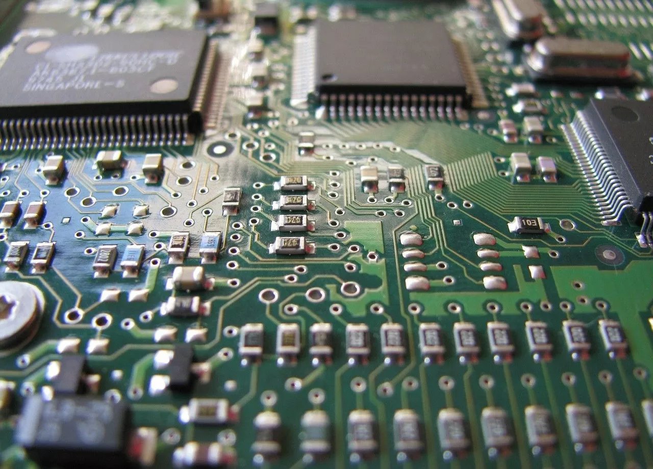
Printed Wiring Boards (PWBs) are a crucial part of electronic devices and contain various features and components that enable the functionality and connectivity of the device. These features and components work together to ensure efficient signal transmission and reliable operation. Here are some common features and components found on PWBs:
Traces: Traces are conductive pathways that connect different components and parts on the PWB. They are typically made of copper and transmit electrical signals between the various parts of the circuit. Traces can vary in width, depending on the current-carrying capacity and signal requirements of the circuit.
Vias: Vias are small holes drilled through the PWB that allow for electrical connections between different layers. They are used to route traces from one layer to another, increasing the routing density and enabling efficient signal transfer. Vias are typically plated with a conductive material to ensure continuity across layers.
Pads: Pads are small areas of copper on the PWB that provide a connection point for component leads or surface mount components. They act as points of contact for soldering or other attachment methods and ensure electrical connectivity between components and the PWB.
SMD Components: Surface Mount Device (SMD) components are mounted directly onto the surface of the PWB, eliminating the need for through-hole soldering. These small components, such as resistors, capacitors, and integrated circuits, have leads designed for soldering onto solder pads. They help save space, reduce manufacturing complexity, and enable miniaturization of electronic devices.
Connectors: Connectors are components that facilitate the connection and disconnection of external devices to the PWB. They come in a variety of types, such as USB ports, HDMI ports, or pin headers, and enable the transfer of power, data, and signals between the PWB and external devices or modules.
ICs and Microprocessors: Integrated Circuits (ICs) and microprocessors are key components on PWBs that provide various functionalities and processing capabilities. These electronic devices are designed to perform specific tasks, such as controlling operations, processing data, or managing communication protocols.
Power Planes: Power planes are dedicated layers within the PWB that provide a continuous supply of power to different parts of the circuit. They help distribute power evenly and efficiently, reducing voltage drop and enhancing the performance and stability of the electronic device.
Ground Planes: Ground planes are also dedicated layers that provide a stable reference voltage or ground connection to the circuit. They help reduce electromagnetic interference and noise, ensuring proper signal integrity and minimizing electrical disturbances in the device.
Solder Mask and Legend: Solder mask is a layer applied over the PWB to protect the copper traces and prevent solder bridges during component assembly. Legend printing is the process of adding text and symbols on the PWB to indicate component reference designators, polarity, and other important information for assembly and troubleshooting purposes.
These are just a few of the many features and components found on PWBs. The combination and arrangement of these elements contribute to the overall functionality and performance of electronic devices, enabling seamless operation and reliable communication.
Challenges and Limitations of PWBs in Electronics
While Printed Wiring Boards (PWBs) are widely used and offer numerous benefits, they also come with their own set of challenges and limitations. These factors must be taken into consideration during the design, manufacturing, and implementation of PWBs in electronic devices. Here are some of the main challenges and limitations:
Complexity: As electronic devices become more advanced and compact, the complexity of the circuitry increases. Designing and manufacturing PWBs with intricate layouts and high component density can pose challenges in terms of signal integrity, thermal management, and manufacturing efficiency. Careful consideration must be given to routing, layer stacking, and electrical isolation.
Signal Integrity: PWBs face challenges in maintaining signal integrity, especially in high-frequency applications. Factors such as trace length, spacing, impedance matching, and electromagnetic interference can impact signal quality and lead to data corruption or transmission errors. Special attention and design techniques are required to ensure proper signal integrity and minimize signal degradation.
Thermal Management: As electronic devices become smaller and more powerful, the issue of heat dissipation becomes critical. The compact nature of PWBs can make it challenging to manage and dissipate heat effectively, leading to potential thermal issues that affect device performance and reliability. Proper heat sinking, placement of heat-generating components, and thermal design considerations are essential to prevent overheating.
Manufacturability: The manufacturing process of PWBs can be complex and requires specialized equipment and expertise. High-density layouts, fine-pitch components, and intricate designs can pose challenges for assembly and soldering processes. Ensuring proper alignment, solder joint quality, and using appropriate manufacturing techniques are crucial to achieving high-quality and reliable PWBs.
Space Limitations: The compact nature of PWBs can become a limiting factor when designing electronic devices with intricate functionality and a large number of components. The limited space on the PWB can lead to constraints in component placement, trace routing, and access for testing and repair. Designers must carefully optimize space utilization to ensure proper functionality and accessibility.
Cost Considerations: While PWBs offer benefits in terms of reliability and scalability, they can also involve significant costs, especially for complex designs, multilayer construction, and advanced manufacturing techniques. Material costs, manufacturing complexity, and additional testing requirements contribute to the overall cost of PWBs. Balancing the performance requirements with cost considerations is crucial in electronic device development.
Environmental Impact: PWBs often contain materials that can have environmental implications if not properly handled. For example, disposing of or recycling electronic waste that includes PWBs requires proper procedures to prevent environmental contamination. Companies must be conscientious about responsible disposal and recycling of PWBs to minimize their environmental impact.
Despite these challenges and limitations, PWBs continue to be an essential component in the field of electronics. By addressing these challenges through innovative design techniques, advanced manufacturing processes, and ongoing research and development, the potential of PWBs can be further optimized to meet the evolving needs of the electronics industry.
PWBs vs. Other Wiring Methods: A Comparison
When it comes to wiring electronic devices, Printed Wiring Boards (PWBs) have become the preferred choice over traditional wiring methods. PWBs offer significant advantages in terms of reliability, efficiency, and performance compared to other wiring approaches. Let’s compare PWBs with other common wiring methods used in electronics:
Point-to-Point Wiring: Point-to-point wiring involves manually connecting components using individual wires. While it can be suitable for simple circuits, it becomes cumbersome and time-consuming as the complexity and number of components increase. PWBs, on the other hand, provide a more efficient and compact solution, eliminating the need for manual wiring and reducing the risk of errors.
Breadboards: Breadboards are temporary platforms used during prototyping. They allow for easy component placement and interconnection without soldering. However, breadboards are not suitable for long-term use as the connections can come loose, leading to unreliable connections. PWBs ensure consistent and sturdy connections, providing long-term reliability and durability for electronic devices.
Wire-Wrapping: Wire-wrapping involves using special wire-wrapping tools to tightly wrap wires around dedicated posts or terminals on a board. While this method provides reliable connections, it is time-consuming and restrictive in terms of reusability and design changes. PWBs allow for easier modifications, upgrades, and maintenance, making them more suitable for complex circuits that require flexibility and adaptability.
Printed Wiring: Printed wiring involves depositing conductive ink onto a non-conductive surface to create circuitry. While this method offers flexibility in circuit design, it typically lacks the durability and reliability of PWBs. PWBs, with their well-defined copper traces and robust construction, provide superior connectivity and long-term performance compared to printed wiring.
Flexible Wiring: Flexible wiring methods, such as ribbon cables and wire harnesses, allow for flexibility in connecting components and routing signals in electronic systems. However, they can be bulky, complex to assemble, and prone to wear and tear over time. Flexible PWBs offer a more compact and reliable solution for applications that require routing flexibility, such as wearable devices or devices with moving parts.
Wireless Connectivity: In some cases, wireless connectivity may replace the need for physical wiring altogether. Though it offers convenience, wireless communication still has limitations like interference and limited range. PWBs are still essential for providing the necessary connections within the electronic device itself and enabling reliable power distribution and signal routing.
Overall, PWBs outperform other wiring methods in terms of reliability, durability, efficiency, and scalability. Their compact design, high-density circuitry, and standardized manufacturing processes make them ideal for mass production and the integration of complex electronics. While other wiring methods may have their specific use cases, PWBs remain the go-to solution for ensuring efficient and reliable operation in a wide range of electronic devices.